
Technical Data
Terminal Block Specifications
Bulletin Number
1492
Additional Resources
These documents contain additional information concerning related products from Rockwell Automation.
You can view or download publications at
http://www.rockwellautomation.com/literature/. To order paper copies of
technical documentation, contact your local Allen-Bradley distributor or Rockwell Automation sales representative.
Topic Page
IEC Screw Type Terminal Blocks 3
IEC Spring Clamp Type Terminal Blocks 24
IEC Terminal Block Accessories 42
NEMA Terminal Blocks 65
NEMA Terminal Block Accessories 69
Power Blocks 78
Resource Description
Industrial Automation Wiring and Grounding Guidelines, publication
1770-4.1 Provides general guidelines for installing a Rockwell Automation industrial system.
Product Certifications website,
http://www.ab.com Provides declarations of conformity, certificates, and other certification details.

3
Rockwell Automation Publication 1492-TD015A-EN-P
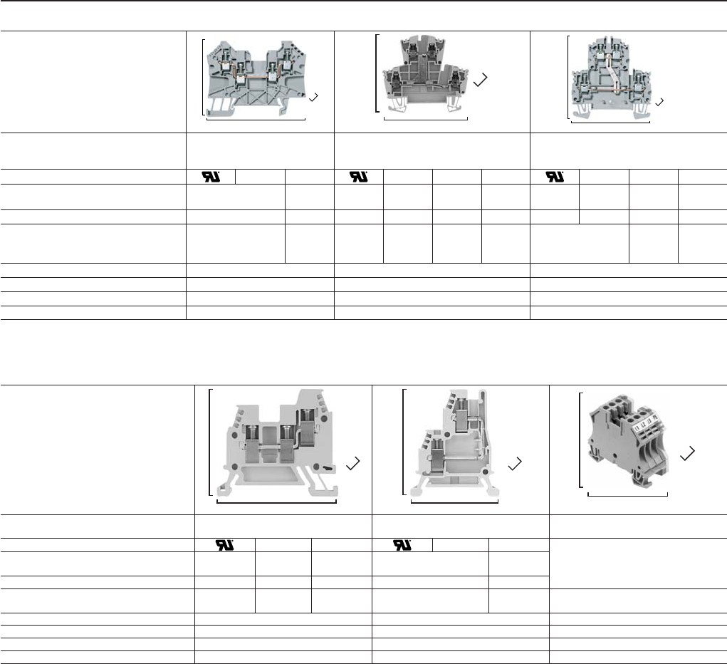
Terminal Block Specifications Screw Type Terminal Blocks
1492-WM3 1492-WM4 1492-WMD1
Dimensions are not intended to be used
for manufacturing purposes.
Note: Height dimension is measured
from top of rail to top of terminal
block.
0.20"
(5 mm)
1.14" (29 mm)
0.97" (24.6 mm)
0.24"
(6 mm)
1.26" (32 mm)
1.10" (28 mm)
0.20"
(5 mm)
1.76" (44.6 mm)
1.35" (34.3 mm)
Specifications Single-circuit mini terminal block. Single-circuit mini terminal block. Two-circuit mini terminal block.
Certifications
IEC CSA ATEX IEC CSA ATEX CSA IEC
Voltage Rating
300V
AC/DC
500V
AC/DC
300V
AC/DC
420V
AC/DC
300V
AC/DC
500V
AC/DC
300V
AC/DC
420V
AC/DC
300V
AC/DC
300V
AC/DC
500V
AC/DC
Maximum Current 15 A 24 A 15 A 24 A 20 A 32 A 20 A 32 A 15 A 15 A 17.5 A
Wire Range (Rated Cross Section)
#30…14
AWG
0.5…2.5
mm
2
#22…14
AWG
2.5 mm
2
#22…12
AWG
0.5…4.0
mm
2
#22…12
AWG
4.0 mm
2
#22…16 AWG
0.5…1.5
mm
2
Wire Strip Length 0.24 in. (6 mm) 0.39 in. (10 mm) 0.35 in. (9 mm)
Recommended Tightening Torque 4.2…4.6 lb•in (0.47....0.52 N•m) 4.7…6.2 lb•in (0.53...0.70 N•m) 4.2…4.6 lb•in (0.47....0.52 N•m)
Density 61 pcs/ft (200/m) 50 pcs/ft (166/m) 61 pcs/ft (200/m)
Housing Temperature Range -40…+195 °F (-40…+90 °C) -40…+195 °F (-40…+90 °C) -40…+195 °F (-40…+90 °C)
1492-WMG3 1492-WMG4
Dimensions are not intended to be used
for manufacturing purposes.
Note: Height dimension is measured
from top of rail to top of terminal
block.
0.24"
(6 mm)
0.84" (21.4 mm)
0.96" (24.5 mm)
0.24"
(6 mm)
1.34" (34 mm)
1.10" (28 mm)
Specifications Single-circuit mini grounding terminal block. Single-circuit mini grounding terminal block.
Certifications IEC
IEC
Maximum Current Grounding Grounding
Wire Range (Rated Cross Section)
#14 AWG (2.5 mm
2
)
#22…12 AWG
0.5…4.0
mm
2
Wire Strip Length 0.31 in. (8 mm) 0.39 in. (10 mm)
Recommended Tightening Torque 6.2 lb•in (0.7 N•m) 5.3 lb•in (0.6 N•m)
Density 50 pcs/ft (166 pcs/m) 50 pcs/ft (166 pcs/m)
Housing Temperature Range — -40…+195 °F (-40…+90 °C)
1492-J3 1492-J4 1492-J6
Dimensions are not intended to be
used for manufacturing purposes.
Note: Height dimension is measured
from top of rail to top of terminal
block.
0.20"
(5.1 mm)
2.36" (60 mm)
1.56" (39.5 mm)
0.24"
(6.1 mm)
2.36" (60 mm)
1.56" (39.5 mm)
0.319"
(8.1 mm)
2.36" (60 mm)
1.56" (39.5 mm)
Specifications Feed-through terminal block Feed-through terminal block Feed-through terminal block
Certifications
CSA IEC ATEX CSA IEC ATEX CSA IEC ATEX
Voltage Rating 600V AC/DC
800V
AC/DC
550V
AC/DC
600V AC/DC
800V
AC/DC
690V
AC/DC
600V AC/DC
800V
AC/DC
550V
AC/DC
Maximum Current 25 A 20 A 24 A 21 A 35 A 25 A 32 A 28 A 50 A 41 A 36 A
Wire Range (Rated Cross Section)
#28…12
AWG
#26…12
AWG
2.5 mm
2
2.5 mm
2
(#20…14
AWG)
#22…10
AWG
#26…10
AWG
4 mm
2
4 mm
2
(#20…12
AWG)
#22…8 AWG
6 mm
2
6 mm
2
(#20…10
AWG)
Wire Strip Length 0.39 in. (10 mm) 0.39 in. (10 mm) 0.47 in. (12 mm)
Recommended Tightening Torque 4.5…7.1 lb•in (0.5…0.8 N•m) 9.0 lb•in (1.0 N•m) 14.2 lb•in (1.6 N•m)
Density 59 pcs/ft (196 pcs/m) 49 pcs/ft (163 pcs/m) 37 pcs/ft (123 pcs/m)
Housing Temperature Range -58…+248 °F (-50…+120 °C) -58…+248 °F (-50…+120 °C) -58…+248 °F (-50…+120 °C)

4
Rockwell Automation Publication 1492-TD015A-EN-P
Screw Type Terminal Blocks Terminal Block Specifications
1492-J10 1492-J16 1492-J35
Dimensions are not intended to be used
for manufacturing purposes.
Note: Height dimension is measured
from top of rail to top of terminal
block.
0.390"
(9.9 mm)
2.36" (60 mm)
1.56" (39.5 mm)
0.472"
(12 mm)
2.36" (60 mm)
2.2" (56 mm)
0.626"
(15.9 mm)
2.36" (60 mm)
2.2" (56 mm)
Specifications Feed-through terminal block Feed-through terminal block Feed-through terminal block
Certifications
CSA IEC ATEX CSA IEC ATEX CSA IEC ATEX
Voltage Rating 600V AC/DC
1000V
AC/DC
550V
AC/DC
600V AC/DC
1000V
AC/DC
690V
AC/DC
1000V
AC/DC
600V
AC/DC
1000V
AC/DC
690V
AC/DC
Maximum Current 65 A 50 A 57 A 50 A 85 A 76 A 66 A 150 A 120 A 125 A 109 A
Wire Range (Rated Cross Section) #18…6 AWG
10 mm
2
10 mm
2
(#16…8
AWG)
#18…4 AWG
16 mm
2
16 mm
2
(#16…6
AWG)
#12…1/
0 AWG
#12…2
AWG
35 mm
2
35 mm
2
(#14…2
AWG)
Wire Strip Length 0.47 in. (12 mm) 0.63 in. (16 mm) 0.70 in. (18 mm)
Recommended Tightening Torque 20.4 lb•in (2.3 N•m) 35.0 lb•in (4.0 N•m) 51.0 lb•in (5.8 N•m)
Density 30 pcs/ft (100 pcs/m) 25 pcs/ft (83 pcs/m) 19 pcs/ft (62 pcs/m)
Housing Temperature Range -58…+248 °F (-50…+120 °C) -58…+248 °F (-50…+120 °C) -58…+248 °F (-50…+120 °C)
1492-J50 1492-J70 1492-J120
Dimensions are not intended to be used for
manufacturing purposes.
Note: Height dimension is measured from top of rail
to top of terminal block.
0.728"
(18.5 mm)
2.89" (73.4 mm)
2.49" (63.3 mm)
0.807"
(20.5 mm)
2.95" (75 mm)
3.10" (78.8 mm)
3.58” (91 mm)
1.06”
(27 mm)
3.31” (84 mm)
Specifications Feed-through terminal block Feed-through terminal block Feed-through terminal block
Certifications
CSA IEC ATEX CSA IEC ATEX CSA IEC
Voltage Rating
1000V
AC/DC
600V
AC/DC
1000V
AC/DC
690V
AC/DC
600V AC/DC
1000V
AC/DC
690V
AC/DC
1000V
AC/DC
Maximum Current 150 A 150 A 126 A 175 A 205 A 192 A 167 A 228 A 220 A 269 A
Wire Range (Rated Cross Section)
#10…
1/0
AWG
#8…
1/0
AWG
50
mm
2
#10…
1/0
AWG
50
mm
2
#6…2/0 AWG
70
mm
2
#8…
2/0
AWG
70
mm
2
#4…
250
MCM
AWG
#4…
4/0
AWG
16…
120
mm
2
Wire Strip Length 0.94 in. (24 mm) 0.87 in. (22 mm) 1.06 in. (27 mm)
Recommended Tightening Torque 31.5 lb•in (3.6 N•m) 87.0 lb•in (9.8 N•m) 141.6 lb•in (16.0 N•m)
Density 16 pcs/ft (54 pcs/m) 14 pcs/ft (48 pcs/m) 11 pcs/ft (37 pcs/m)
Housing Temperature Range -58…+248 °F (-50…+120 °C) -58…+248 °F (-50…+120 °C) -58...+248 °F (-50...+120 °C)

5
Rockwell Automation Publication 1492-TD015A-EN-P
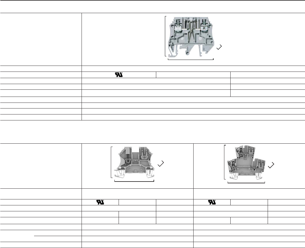
Terminal Block Specifications Screw Type Terminal Blocks
1492-W3 1492-W4 1492-W6
Dimensions are not intended to be used
for manufacturing purposes.
Note: Height dimension is measured
from top of rail to top of terminal
block.
0.20"
(5 mm)
1.78" (45.3 mm)
1.38" (35 mm)
0.24"
(6 mm)
1.78" (45.3 mm)
1.38" (35 mm)
0.28"
(7 mm)
1.87" (47.6 mm)
1.61" (41 mm)
Specifications Single-circuit terminal block. Single-circuit terminal block. Single-circuit terminal block.
Certifications
IEC CSA ATEX IEC CSA ATEX IEC CSA
Voltage Rating
600V
AC/DC
800V
AC/DC
600V
AC/DC
550V
AC/DC
600V
AC/DC
800V
AC/DC
600V
AC/DC
550V
AC/DC
600V
AC/DC
800V
AC/DC
600V
AC/DC
Maximum Current 20 A 24 A 20 A 24 A 30 A 32 A 30 A 32 A 40 A 41 A 40 A
Wire Range (Rated Cross Section)
#30…14
AWG
0.5…2.5
mm
2
#22…14
AWG
2.5 mm
2
#22…10
AWG
0.5…4.0
mm
2
#22…10
AWG
4.0 mm
2
#22…10
AWG
0.5…6.0
mm
2
#22…10
AWG
Wire Strip Length 0.39 in. (10 mm) 0.35 in. (9 mm) 0.47 in. (12 mm)
Recommended Tightening Torque 5.0…5.6 lb•in (0.6 N•m) 5.0…5.6 lb•in (0.6 N•m) 5.6…6.8 lb•in (0.7 N•m)
Density 61 pcs/ft (200 pcs/m) 50 pcs/ft (166 pcs/m) 43 pcs/ft (142 pcs/m)
Housing Temperature Range -40…+195 °F (-40…+90 °C) -40…+195 °F (-40…+90 °C) -40…+195 °F (-40…+90 °C)
1492-W10 1492-W16S
Dimensions are not intended to be used
for manufacturing purposes.
Note: Height dimension is measured
from top of rail to top of terminal
block.
0.31"
(8 mm)
1.87" (47.6 mm)
1.61" (41 mm)
0.43"
(11 mm)
1.87" (47.6 mm)
1.61" (41 mm)
Specifications Single-circuit terminal block. Single-circuit terminal block.
Certifications
IEC CSA ATEX IEC CSA ATEX
Voltage Rating 600V AC/DC 800V AC/DC 600V AC/DC 550V AC/DC 600V AC/DC 800V AC/DC 600V AC/DC 550V AC/DC
Maximum Current 50 A 57 A 50 A 50 A 85 A 76 A 85 A 76 A
Wire Range (Rated Cross Section) #22…8 AWG
10 mm
2
#22…8 AWG
0.5…10 mm
2
#14…4 AWG
16 mm
2
#14…4 AWG
2.5…16 mm
2
Wire Strip Length 0.51 in. (13 mm) 0.51 in. (13 mm)
Recommended Tightening Torque 12.2…13.4 lb•in (1.4 N•m) 18…20 lb•in (2.1 N•m)
Density 38 pcs/ft (125 pcs/m) 27 pcs/ft (90 pcs/m)
Housing Temperature Range -40…+195 °F (-40…+90 °C) -40…+195 °F (-40…+90 °C)

6
Rockwell Automation Publication 1492-TD015A-EN-P
Screw Type Terminal Blocks Terminal Block Specifications
1492-JD3 1492-JD4 1492-JT3M
Dimensions are not intended to be used
for manufacturing purposes.
Note: Height dimension is measured
from top of rail to top of terminal
block.
0.20"
(5.1 mm)
2.72" (69 mm)
2.19" (55.5 mm)
0.24"
(6.1 mm)
2.39" (60.7 mm)
2..24" (57 mm)
0.24"
(6.1 mm)
3.47" (88 mm)
2..22" (56.5 mm)
Specifications
Two-level, two-circuit feed-through
terminal block
Two-level, two-circuit feed-through terminal
block
Three-level, three-circuit
terminal block with ground point
Certifications
CSA IEC ATEX CSA IEC ATEX CSA IEC
Voltage Rating
600V
AC/DC
300V
AC/DC
400V
AC/DC
275V
AC/DC
600V
AC/DC
300V
AC/DC
800V
AC/DC
550V
AC/DC
300V AC/DC
400V
AC/DC
Maximum Current 20 A 10 A 24 A 21 A 35 A 30 A 32 A 28 A 10 A 24 A
Wire Range (Rated Cross Section)
#22…
12
AWG
26…12
AWG
2.5 mm
2
2.5 mm
2
(20…
14 AWG)
#26…10 AWG
0.5…4
mm
2
4 mm
2
(20…12
AWG)
#22…12
AWG
#26…10
AWG
0.5…2.5
mm
2
Wire Strip Length 0.39 in. (10 mm) 0.315 in. (8 mm) 0.28 in. (7 mm)
Recommended Tightening Torque 4.5…7.1 lb•in (0.5…0.8 N•m) 4.5 lb•in (0.5 N•m) 4.4 lb•in (0.5 N•m)
Density 59 pcs/ft (196 pcs/m) 49 pcs/ft (163 pcs/m) 49 pcs/ft (163 pcs/m)
Housing Temperature Range -58…+248 °F (-50…+120 °C) -58…+248 °F (-50…+120 °C) -58…+248 °F (-50…+120 °C)
1492-J2Q 1492-J3TW 1492-J4TW
Dimensions are not intended to be used
for manufacturing purposes.
Note: Height dimension is measured
from top of rail to top of terminal
block.
0.20"
(5.1 mm)
2.36" (60 mm)
1.56" (39.5 mm)
0.20"
(5.1 mm)
2.36" (60 mm)
1.56" (39.5 mm)
0.24"
(6.1 mm)
2.49" (63 mm)
1.81" (46 mm)
Specifications
Feed-through terminal block with 2
connection points on each side
Feed-through terminal block with 3 connection
points, 2 on one side
Feed-through terminal block with 3
connection points, 2 on one side
Certifications
CSA IEC CSA IEC ATEX CSA IEC
Voltage Rating 300V AC/DC
800V
AC/DC
300V AC/DC
800V
AC/DC
550V
AC/DC
600V AC/DC
500V
AC/DC
Maximum Current 25 A 10 A 17.5 A — 30 A 32 A
Maximum
Current
Single Side — 10 A 15 A 17.5 A 15 A — — —
Twin Side — 20 A 24 A 21 A — — —
Wire Range
(Rated Cross
Section)
Single Side
#22…12
AWG
#26…12
AWG
1.5 mm
2
#22…12
AWG
26…12
AWG
2.5 mm
2
2.5 mm
2
(#20…14
AWG)
#30…10 AWG
4 mm
2
Twin Side —
#22…12
AWG
26…12
AWG
1.5 mm
2
1.5 mm
2
(#20…16
AWG)
Wire Strip Length 0.28 in. (7 mm)
Single Side: 0.39 in. (10 mm)
0.39 in. (10 mm)
Twin Side: 0.26 in. (7 mm)
Recommended Tightening Torque 4.5 lb•in (0.5 N•m)
Single Side: 7.0 lb•in (0.8 N•m)
6.2 lb•in (0.7 N•m)
Twin Side:4.5 lb•in (0.5 N•m)
Density 59 pcs/ft (196 pcs/m) 59 pcs/ft (196 pcs/m) 59 pcs/ft (196 pcs/m)
Housing
Temperature
Range
Insulation Temperature
Range
-58…+248 °F (-50…+120 °C) -58…+248 °F (-50…+120 °C) -58…+248 °F (-50…+120 °C)
7
Rockwell Automation Publication 1492-TD015A-EN-P
Terminal Block Specifications Screw Type Terminal Blocks
1492-J4Q 1492-JD3C 1492-JD4C
Dimensions are not intended to be used
for manufacturing purposes.
Note: Height dimension is measured
from top of rail to top of terminal
block.
0.24"
(6.1 mm)
2.72" (69 mm)
1.81" (46 mm)
0.20"
(5.1 mm)
2.72" (69 mm)
2.19" (55.5 mm)
0.24"
(6.1 mm)
2.39" (60.7 mm)
2..24" (57 mm)
Specifications
Single-level feed-through
terminal block with 2
connection points on each side
Two-level feed-through terminal block with
commoning bar
Two-level feed-through terminal block with
commoning bar
Certifications
CSA IEC CSA IEC ATEX CSA IEC ATEX
Voltage Rating 600V AC/DC
500V
AC/DC
600V
AC/DC
300V
AC/DC
400V
AC/DC
275V
AC/DC
600V
AC/DC
300V
AC/DC
400V
AC/DC
550V
AC/DC
Maximum Current 30 A 32 A 20 A 10 A 24 A 21 A 35 A 30 A 32 A 28 A
Wire Range (Rated Cross Section) #30…10 AWG
0.5…4
mm
2
#22…12
AWG
#26…12
AWG
2.5 mm
2
2.5 mm
2
(20…
14 AWG)
#26…10 AWG
0.5…4
mm
2
4 mm
2
(20…12
AWG)
Wire Strip Length 0.39 in. (10 mm) 0.39 in. (10 mm) 0.28 in. (7 mm)
Recommended Tightening Torque 6.2 lb•in (0.7 N•m) 4.5…7.1 lb•in (0.5…0.8 N•m) 4.5 lb•in (0.5 N•m)
Density 49 pcs/ft (163 pcs/m) 59 pcs/ft (196 pcs/m) 49 pcs/ft (163 pcs/m)
Housing Temperature Range -58…+248 °F (-50…+120 °C) -58…+248 °F (-50…+120 °C) -58…+248 °F (-50…+120 °C)
1492-W4TW 1492-WR3 1492-J4M
Dimensions are not intended to be used
for manufacturing purposes.
Note: Height dimension is measured
from top of rail to top of terminal
block.
0.24"
(6 mm)
2.05" (52.1 mm)
1.64" (41.6 mm)
0.20"
(5 mm)
1.78" (45.3 mm)
1.99" (50.5 mm)
0.965"
(24.5 mm)
2.36" (60 mm)
1.56" (39.5 mm)
Specifications
Feed-through terminal block with 3
connection points, 2 on one side
Single-circuit terminal block with
terminals on common side.
Motor connection terminal block
cluster with 3 feeds and ground
Certifications
CSA IEC CSA IEC
Certifications on
individual blocks
(1492-J4, JG4)
Voltage Rating
600V
AC/DC
600V
AC/DC
800V
AC/DC
300V AC/DC
500V
AC/DC
Maximum Current 30 A 20 A 32 A 15 A 15 A
Wire Range (Rated Cross Section)
#18…10
AWG
#22…12
AWG
0.5…4 mm
2
#22…14 AWG
0.5…2.5
mm
2
#22…10 AWG
4 mm
2
Wire Strip Length 0.35 in. (9 mm) 0.39 in. (10 mm) 0.39 in. (10 mm)
Recommended Tightening Torque 5.0…5.6 lb•in (0.6 N•m) 5.0…5.6 lb•in (0.6 N•m) 9.0 lb•in (1.0 N•m)
Density 50 pcs/ft (166 pcs/m) 61 pcs/ft (200 pcs/m) 12 pcs/ft (40 pcs/m)
Housing Temperature Range -40…+195 °F (-40…+90 °C) -40…+195 °F (-40…+90 °C) -58…+248 °F (-50…+120 °C)
8
Rockwell Automation Publication 1492-TD015A-EN-P
Screw Type Terminal Blocks Terminal Block Specifications
1492-J4CTB
Dimensions are not intended to be used
for manufacturing purposes.
Note: Height dimension is measured
from top of rail to top of terminal
block.
0.24"
(6.1 mm)
2.16" (55 mm)
1.67" (42.5 mm)
Specifications Single-level feed through block with circuit-break test/measurement plug capability
Certifications
CSA IEC
Voltage Rating 300V AC/DC 500V AC/DC
Maximum Current 8 A 6 A
Wire Range (Rated Cross Section) #26…10 AWG
0.5…4 mm
2
Wire Strip Length 0.394 in. (10 mm)
Recommended Tightening Torque 4.4…7.1 lb•in (0.5…0.8 N•m)
Density 49 pcs/ft (163 pcs/m)
Housing Temperature Range -58…+248 °F (-50…+120 °C)
1492-J3F 1492-JD3F
Dimensions are not intended to be used
for manufacturing purposes.
Note: Height dimension is measured
from top of rail to top of terminal
block.
0.20"
(5.1 mm)
2.36" (60 mm)
1.56" (39.5 mm)
0.20"
(5.1 mm)
2.74" (69.5 mm)
2.19" (55.5 mm)
Specifications
Feed-through terminal block with stab connections on
one side
Two-level, two-circuit feed-through terminal block with
stab connections on one side
Certifications
CSA IEC CSA IEC
Voltage Rating 300V AC/DC 500V AC/DC 300V AC/DC 400V AC/DC
Maximum Current 16 A 10 A 16 A (2 x 8) 10 A 16 A (2 x 8)
Wire Range (Rated Cross Section) #22…12 AWG #26…12 AWG
2.5 mm
2
#22…12 AWG #26…12 AWG
2.5 mm
2
Wire Strip Length 0.39 in. (10 mm) 0.39 in. (10 mm)
Recommended Tightening Torque 4.5…7.1 lb•in (0.5…0.8 N•m) 4.5…7.1 lb•in (0.5…0.8 N•m)
Density
59 pcs/ft (196 pcs/m) 59 pcs/ft (196 pcs/m)
Housing Temperature Range -58…+248 °F (-50…+120 °C) -58…+248 °F (-50…+120 °C)

9
Rockwell Automation Publication 1492-TD015A-EN-P
Terminal Block Specifications Screw Type Terminal Blocks
1492-JG2Q 1492-JG3 1492-JG3TW
Dimensions are not intended to be used
for manufacturing purposes.
Note: Height dimension is measured
from top of rail to top of terminal
block.
0.20"
(5.1 mm)
2.36" (60 mm)
1.56" (39.5 mm)
0.20"
(5.1 mm)
2.36" (60 mm)
1.56" (39.5 mm)
0.20"
(5.1 mm)
2.36" (60 mm)
1.56" (39.5 mm)
Specifications
Feed-through grounding
terminal block with 2
connection points on each side
Feed-through grounding terminal block
Feed-through grounding terminal block
with 3 connection points, 2 on one side
Certifications
CSA IEC CSA IEC ATEX CSA IEC ATEX
Voltage Rating ———————————
Maximum Current Grounding Grounding Grounding
Wire Range
(Rated Cross Section)
#22…14 AWG
1.5 mm
2
#22…12 AWG
2.5 mm
2
2.5 mm
2
(#20…14
AWG)
Single Side:
#22…12 AWG 2.5 mm
2
2.5 mm
2
(#20…14
AWG)
Twin Side:
#26…12 AWG 1.5 mm
2
1.5
mm
2
(#20
…16
AWG)
Wire Strip Length 0.28 in. (7 mm) 0.39 in. (10 mm)
Single Side: 0.39 in. (10 mm)
Twin Side: 0.28 in. (7 mm)
Recommended Tightening Torque 5.0 lb•in (0.6 N•m) 7.1 lb•in (0.8 N•m) Single Side: 7.1 lb•in (0.8 N•m)
Mounting Torque — Center Screw 3.5…5.3 lb•in (0.4…0.6 N•m) 3.5…6.2 lb•in (0.4…0.6 N•m) Twin Side: 4.5 lb•in (0.5 N•m)
Density 59 pcs/ft (196 pcs/m) 59 pcs/ft (196 pcs/m) 59 pcs/ft (196 pcs/m)
Housing Temperature Range -58…+248 °F (-50…+120 °C) -58…+248 °F (-50…+120 °C) -58…+248 °F (-50…+120 °C)
1492-WTF3… 1492-WTS3…
Dimensions are not intended to be used
for manufacturing purposes.
Note: Height dimension is measured
from top of rail to top of terminal
block.
0.20"
(5.1 mm)
3.54" (89.9 mm)
1.74" (44.1 mm)
0.20"
(5.1 mm)
2.66" (67.6 mm)
1.74" (44.1 mm)
Specifications Three-circuit terminal block. Three-level sensor block.
Certifications
CSA IEC CSA IEC
Voltage Rating 300V AC/DC 250V AC/DC 300V AC/DC 250V AC/DC
Maximum Current 10 A 24 A 10 A 24 A
Wire Range (Rated Cross Section) #26…14 AWG
0.5…2.5mm
2
#26…14 AWG
0.5…2.5 mm
2
Recommended Tightening Torque 4.2…4.6 lb•in (0.5 N•m) 4.2…4.6 lb•in (0.5 N•m)
Density 60 pcs/ft (197 pcs/m) 60 pcs/ft (197 pcs/m)
Housing Temperature Range -40…+195 °F (-40…+90 °C) -40…+195 °F (-40…+90 °C)
Indicator Type
WTF3/WTS3
No indicator No indicator
WTF3LP/WTS3LP Red LED for PNP devices (10…50V) Red LED for PNP devices (10…50V)
WTF3LN/WTS3LN Red LED for NPN devices (10…50V) Red LED for NPN devices (10…50V)
Leakage Current
WTF3/WTS3
——
WTF3LP/WTS3LP 2.69 mA @ 50V 2.69 mA @ 50V
WTF3LN/WTS3LN 2.69 mA @ 50V 2.69 mA @ 50V
Wire Strip Length 0.31 in. (8 mm) 0.31 in. (8 mm)

10
Rockwell Automation Publication 1492-TD015A-EN-P
Screw Type Terminal Blocks Terminal Block Specifications
1492-JG6 1492-JG10
Dimensions are not intended to be
used for manufacturing purposes.
Note: Height dimension is measured
from top of rail to top of terminal
block.
0.319"
(8.1 mm)
2.36" (60 mm)
1.56" (39.5 mm)
0.394"
(10 mm)
2.36" (60 mm)
1.56" (39.5 mm)
Specifications Feed-through grounding terminal block Feed-through grounding terminal block
Certifications
CSA IEC ATEX CSA IEC ATEX
Voltage Rating ————————
Maximum Current Grounding Grounding
Wire Range (Rated Cross Section) #22…8 AWG
6 mm
2
6 mm
2
(#20…10
AWG)
#16…6 AWG
10 mm
2
10 mm
2
(#16…8
AWG)
Wire Strip Length 0.47 in. (12 mm) 0.47 in. (12 mm)
Recommended Tightening Torque 14.2 lb•in (1.6 N•m) 20.4 lb•in (2.3 N•m)
Mounting Torque — Center Screw 4.4…8.9 lb•in (0.5…1.0 N•m) 4.4…8.9 lb•in (0.5…1.0 N•m)
Density 37 pcs/ft (123 pcs/m) 30 pcs/ft (100 pcs/m)
Housing Temperature Range -58…+248 °F (-50…+120 °C) -58…+248 °F (-50…+120 °C)
1492-JG4 1492-JG4TW 1492-JG4Q
Dimensions are not intended to be used
for manufacturing purposes.
Note: Height dimension is measured
from top of rail to top of terminal
block.
0.24"
(6.1 mm)
2.36" (60 mm)
1.56" (39.5 mm)
0.24"
(6.1 mm)
2.49" (63 mm)
1.81" (46 mm)
0.24"
(6.1 mm)
2.72" (69 mm)
1.81" (46 mm)
Specifications Feed-through grounding terminal block
Single-level grounding terminal
block with 3 connection points, 2
on one side
Single-level grounding terminal
block with two connection points
on each sides
Certifications
CSA IEC ATEX CSA IEC CSA IEC
Voltage Rating ———— — —
Maximum Current Grounding Grounding Grounding
Wire Range (Rated Cross Section) #22…10 AWG
4 mm
2
4 mm
2
(#20…12
AWG)
#30…10 AWG
0.5…4
mm
2
#30…10 AWG
0.5…4
mm
2
Wire Strip Length 0.39 in. (10 mm) 0.394 in. (10 mm) 0.394 in. (10 mm)
Recommended Tightening Torque 9 lb-in (1.0 N•m) 6.2 lb•in (0.7 N•m) 6.2 lb•in (0.7 N•m)
Mounting Torque - Center Screw 4.4…7.1 lb•in (0.5…0.8 N•m) — —
Density 49 pcs/ft (163 pcs/m) 49 pcs/ft (163 pcs/m) 49 pcs/ft (163 pcs/m)
Housing Temperature Range -58…+248 °F (-50…+120 °C) -58…+248 °F (-50…+120 °C) -58…+248 °F (-50…+120 °C)
1492-JG16 1492-JG35 1492-JG50
Dimensions are not intended to be used
for manufacturing purposes.
Note: Height dimension is measured
from top of rail to top of terminal
block.
0.472"
(12 mm)
2.36" (60 mm)
2.20" (56 mm)
0.56"
(16 mm)
2.36" (60 mm)
2.48" (63 mm)
0.728"
(18.5 mm)
2.89" (73.4 mm)
2.49" (63.3 mm)
Specifications Feed-through grounding terminal block Feed-through grounding terminal block Feed-through grounding terminal block
Certifications
CSA IEC ATEX CSA IEC ATEX CSA IEC ATEX
Voltage Rating ————————————
Maximum Current Grounding Grounding Grounding
Wire Range (Rated Cross Section) #24…4 AWG
16 mm
2
16 mm
2
(#16…6
AWG)
#12…1
AWG
#12…2
AWG
35 mm
2
35 mm
2
(#14…2
AWG)
#10…
1/0
AWG
#14…
1/0
AWG
50 mm
2
50 mm
2
(10…1/0
AWG)
Wire Strip Length 0.63 in. (16 mm) 0.70 in. (18 mm) 0.94 in. (24 mm)
Recommended Tightening Torque 35.0 lb•in (4.0 N•m) 51.0 lb•in (5.8 N•m) 31.5 lb•in (3.6 N•m)
Mounting Torque — Center Screw 10.6…21.2 lb•in (1.2…2.4 N•m) 10.6…21.2 lb•in (1.2…2.4 N•m) 17.7…35.4 lb•in (2.0…4.0 N•m)
Density 25 pcs/ft (83 pcs/m) 19 pcs/ft (62 pcs/m) 16 pcs/ft (54 pcs/m)
Housing Temperature Range -58…+248 °F (-50…+120 °C) -58…+248 °F (-50…+120 °C) -58…+248 °F (-50…+120 °C)

11
Rockwell Automation Publication 1492-TD015A-EN-P
Terminal Block Specifications Screw Type Terminal Blocks
1492-JG70 1492-JG120 1492-JDG3
Dimensions are not intended to be used
for manufacturing purposes.
Note: Height dimension is measured
from top of rail to top of terminal
block.
0.807"
(20.5 mm)
2.95" (75 mm)
3.10" (78.8 mm)
3.58” (91 mm)
1.06”
(27 mm)
3.31” (84 mm)
0.20"
(5.1 mm)
2.72" (69 mm)
2.19" (55.5 mm)
Specifications Feed-through grounding terminal block
Feed-through grounding terminal
block
Two-circuit terminal block with one
feed-through and one grounding circuit
Certifications
CSA IEC ATEX CSA IEC CSA IEC ATEX
Voltage Rating — —
300V
AC/DC
400V
AC/DC
275V
AC/DC
Maximum Current Grounding — 20 A 24 A 21 A
Wire Range (Rated Cross Section) #6…2/0 AWG
70 mm
2
70 mm
2
(#8…2/0
AWG)
#4…3/0 AWG
#4…4/0
AWG
16...95
mm
2
#22…12 AWG
2.5 mm
2
2.5 mm
2
(#20…14
AWG)
Wire Strip Length 0.87 in. (22 mm) 1.06 in. (27 mm) 0.39 in. (10 mm)
Recommended Tightening Torque 87.0 lb•in (9.8 N•m) 88.5 lb•in (10 N•m) 4.5…7.1 lb•in. (0.5…0.8 N•m)
Mounting Torque — Center Screw 17.7…35.4 lb•in (2.0…4.0 N•m) — —
Density 14 pcs/ft (48 pcs/m) 11 pcs/ft (37 pcs/m) 59 pcs/ft (196 pcs/m)
Housing Temperature Range -58…+248 °F (-50…+120 °C) -58…+248 °F (-50…+120 °C) -58…+248 °F (-50…+120 °C)
1492-JDG3C 1492-JDG4 1492-JDG4C
Dimensions are not intended to be used
for manufacturing purposes.
Note: Height dimension is measured
from top of rail to top of terminal
block.
0.20"
(5.1 mm)
2.72" (69 mm)
2.19" (55.5 mm)
0.24"
(6.1 mm)
2.39" (60.7 mm)
2.52" (64.1 mm)
Specifications
Two-level grounding terminal block
with commoning bar
Two-circuit terminal block with one
feed-through and one grounding
Two-level grounding terminal block
with commoning bar
Certifications
CSA IEC ATEX CSA IEC ATEX CSA IEC ATEX
Voltage Rating —
600V
AC/DC
300V
AC/DC
800V
AC/DC
550V
AC/DC
—
Maximum Current Grounding 35 A 30 A 32 A 28 A Grounding
Wire Range (Rated Cross Section)
#22…12
AWG
#26…12
AWG
2.5 mm
2
2.5 mm
2
(#20…1
4 AWG)
#26…10 AWG
4 mm
2
4 mm
2
#26…10 AWG
4 mm
2
4 mm
2
Wire Strip Length 0.39 in. (10 mm) 0.31 in. (8 mm) 0.31 in. (8 mm)
Recommended Tightening Torque 4.5…7.1 lb•in (0.5…0.8 N•m) 4.5…8.8 lb•in (0.5…1.0 N•m) 4.5…8.8 lb•in (0.5…1.0 N•m)
Mounting Torque — Center Screw — — —
Density 59 pcs/ft (196 pcs/m) 49 pcs/ft (163 pcs/m) 49 pcs/ft (163 pcs/m)
Housing Temperature Range -58…+248 °F (-50…+120 °C) -58…+248 °F (-50…+120 °C) -58…+248 °F (-50…+120 °C)

12
Rockwell Automation Publication 1492-TD015A-EN-P
Screw Type Terminal Blocks Terminal Block Specifications
1492-WG4 1492-WG6 1492-WG10S
Dimensions are not intended to be used
for manufacturing purposes.
Note: Height dimension is measured
from top of rail to top of terminal
block.
0.24"
(6 mm)
1.89" (48 mm)
1.38" (35 mm)
0.28"
(7 mm)
1.89" (48 mm)
1.61" (41 mm)
0.31"
(8 mm)
1.89" (48 mm)
1.61" (41 mm)
Specifications
Single-circuit grounding terminal
block.
Single-circuit grounding terminal
block.
Single-circuit grounding terminal
block.
Certifications
IEC CSA ATEX IEC CSA ATEX CSA IEC
Voltage Rating ———————— — — —
Maximum Current Grounding Grounding Grounding
Wire Range (Rated Cross Section)
#22…12
AWG
4 mm
2
#22…12
AWG
4 mm
2
#22…10
AWG
6 mm
2
#22…10
AWG
6 mm
2
#22…8
AWG
#22…8
AWG
10 mm
2
Wire Strip Length 0.43 in. (11 mm) 0.47 in. (12 mm) 0.43 in. (11 mm)
Recommended Tightening Torque 5.6…6.8 lb•in (0.7 N•m) 5.6…6.8 lb•in (0.7 N•m) 7.1 lb•in (0.8 N•m)
Density 50 pcs/ft (166 pcs/m) 43 pcs/ft (142 pcs/m) 38 pcs/ft (125 pcs/m)
Housing Temperature Range -40…+195 °F (-40…+90 °C) -40…+195 °F (-40…+90 °C) -40…+195 °F (-40…+90 °C)
1492-WG16S
Dimensions are not intended to be used
for manufacturing purposes.
Note: Height dimension is measured
from top of rail to top of terminal
block.
0.51"
(13 mm)
2.14" (54.3 mm)
1.6" (41 mm)
Specifications Single-circuit grounding terminal block.
Certifications
CSA IEC
Voltage Rating — — —
Maximum Current Grounding
Wire Range (Rated Cross Section) #14…4 AWG
2.5…16 mm
2
Wire Strip Length 0.51 in. (13 mm)
Recommended Tightening Torque 18…20 lb•in (2.1 N•m)
Center Screw Mounting Torque 10.6 lb•in (1.2 N•m)
Density 27 pcs/ft (90 pcs/m)
Housing Temperature Range -40…+195 °F (-40…+90 °C)

13
Rockwell Automation Publication 1492-TD015A-EN-P
Terminal Block Specifications Screw Type Terminal Blocks
1492-JKD3 1492-JKD3TP 1492-JKD4
Dimensions are not intended to be used
for manufacturing purposes.
Note: Height dimension is measured
from top of rail to top of terminal
block.
0.20"
(5.1 mm)
2.36" (60 mm)
1.88" (47 mm)
0.20"
(5.1 mm)
2.36" (60 mm)
1.88" (47 mm)
Specifications
Feed through terminal block with knife
disconnect
Feed-through terminal block with knife
disconnect and test screws
Feed-through terminal block with knife
disconnect
Certifications
CSA IEC CSA IEC CSA IEC
Voltage Rating 300V AC/DC
500V
AC/DC
300V AC/DC
500V
AC/DC
600V
AC/DC
300V
AC/DC
400V
AC/DC
Maximum Current 10 A 24 A 10 A 24 A 22 A 10 A 32 A
Wire Range (Rated Cross Section) #22…12 AWG
2.5 mm
2
#22…12 AWG
2.5 mm
2
#22…10 AWG
0.05…4.0
mm
2
Fuse Size (Dummy Fuse Supplied) — — —
Wire Strip Length 0.39 in. (10 mm) 0.39 in. (10 mm) 0.512 in. (13 mm)
Recommended Tightening Torque 7.1 lb•in. (0.8 N•m) 7.1 lb•in. (0.8 N•m) 9.0 lb•in. (1.0 N•m)
Density 49 pcs/ft (163 pcs/m) 49 pcs/ft (163 pcs/m) 49 pcs/ft (163 pcs/m)
Housing Temperature Range –58…+248 °F (–50…+120 °C) –58…+248 °F (–50…+120 °C) –58…+248 °F (–50…+120 °C)
1492-JKD4TW 1492-JKD4Q 1492-H7
Dimensions are not intended to be used
for manufacturing purposes.
Note: Height dimension is measured
from top of rail to top of terminal
block.
0.24"
(6.1 mm)
2.48" (63 mm)
1.81" (46 mm)
0.24"
(6.1 mm)
2.72" (69 mm)
1.81" (46 mm)
0.36"
(9.1 mm)
3.20" (81.3 mm)
1.85" (47 mm)
Specifications
Feed-through terminal block with knife
disconnect; 3 connection points, 2 on
one side
Feed-through terminal block with knife
disconnect; 2 connection points on
each side
Handle-style isolating terminal block
Certifications
CSA IEC CSA IEC CSA IEC
Voltage Rating 600V AC/DC
500V
AC/DC
600V AC/DC
500V
AC/DC
300V
AC/DC
300V
AC/DC
500V
AC/DC
Maximum Current 25 A 30 A 25 A 30 A 15 A 15 A 15 A
Wire Range (Rated Cross Section) #30…10 AWG
0.5…4
mm
2
#30…10 AWG
0.5…4
mm
2
#30…10 AWG
0.5…4.0
mm
2
Fuse Size (Dummy Fuse Supplied) — — 1/4 x 1-1/4 in.
Wire Strip Length 0.39 in. (10 mm) 0.39 in. (10 mm) 0.38 in. (9.7 mm)
Recommended Tightening Torque 6.2 lb•in (0.7 N•m) 6.2 lb•in (0.7 N•m) 7.1 lb•in (0.8 N•m)
Density 49 pcs/ft (163 pcs/m) 49 pcs/ft (163 pcs/m) 33 pcs/ft (109 pcs/m)
Housing Temperature Range -58…+248 °F (-50…+120 °C) -58…+248 °F (-50…+120 °C) -40…+221 °F (-40…+105 °C)

14
Rockwell Automation Publication 1492-TD015A-EN-P
Screw Type Terminal Blocks Terminal Block Specifications
1492-J3P 1492-J3PTP 1492-JD3P
Dimensions are not intended to be used
for manufacturing purposes.
Note: Height dimension is measured
from top of rail to top of terminal
block.
0.20"
(5.1 mm)
2.36" (60 mm)
1.56" (39.5 mm)
0.20"
(5.1 mm)
2.36" (60 mm)
1.56" (39.5 mm)
0.20"
(5.1 mm)
2.85" (72.5 mm)
2.33" (59.3 mm)
Specifications
Selectable component plug-in
terminal block
Selectable component plug-in
terminal block with test plug socket
Two Circuit selectable component
plug-in terminal block
Certifications
CSA IEC CSA IEC CSA IEC
Voltage Rating
600V
AC/DC
300V
AC/DC
500V
AC/DC
300V AC/DC
500V
AC/DC
300V AC/DC
500V
AC/DC
Maximum Current 20 A 10 A 24 A 20 A 10 A 24 A 20 A 24 A
Wire Range (Rated Cross Section) #30…12 AWG
2.5 mm
2
#30…12 AWG
2.5 mm
2
#24…12
AWG
#30…12
AWG
2.5 mm
2
Wire Strip Length 0.39 in. (10 mm) 0.39 in. (10 mm) 0.31 in. (8 mm)
Recommended Tightening Torque 4.4 lb•in (0.5 N•m) 4.4 lb•in (0.5 N•m) 4.4 lb•in (0.5 N•m)
Density 59 pcs/ft (196 pcs/m) 59 pcs/ft (196 pcs/m) 59 pcs/ft (196 pcs/m)
Housing Temperature Range -58…+248 °F (-50…+120 °C) -58…+248 °F (-50…+120 °C) -58…+248 °F (-50…+120 °C)
1492-JD3PTP 1492-JD3PSS 1492-JD3PSSTP
Dimensions are not intended to be used
for manufacturing purposes.
Note: Height dimension is measured
from top of rail to top of terminal
block.
0.20"
(5.1 mm)
2.85" (72.5 mm)
2.33" (59.3 mm)
0.20"
(5.1 mm)
2.85" (72.5 mm)
2.33" (59.3 mm)
0.20"
(5.1 mm)
2.85" (72.5 mm)
2.33" (59.3 mm)
Specifications
Two-circuit selectable component
plug-in terminal block with test plug
socket
Two-circuit selectable component
plug-in terminal block with internal
surge suppressor
Two-circuit selectable component
plug-in terminal block with internal
surge suppressor and test plug socket
Certifications
CSA IEC CSA IEC CSA IEC
Voltage Rating 300V AC/DC
500V
AC/DC
300V AC/DC 115V AC 300V AC/DC
115V
AC/DC
Maximum Current 20 A 24 A 20 A 24 A 20 A 24 A
Wire Range (Rated Cross Section)
#24…12
AWG
#30…12
AWG
2.5 mm
2
#24…12
AWG
#30…12
AWG
2.5 mm
2
#24…12
AWG
#30…12
AWG
2.5 mm
2
Wire Strip Length 0.31 in. (8 mm) 0.31 in. (8 mm) 0.31 in. (8 mm)
Recommended Tightening Torque 4.4 lb•in (0.5 N•m) 4.4 lb•in (0.5 N•m) 4.4 lb•in (0.5 N•m)
Density 59 pcs/ft (196 pcs/m) 59 pcs/ft (196 pcs/m) 59 pcs/ft (196 pcs/m)
Housing Temperature Range -58…+248 °F (-50…+120 °C) -58…+248 °F (-50…+120 °C) –58…+248 °F (–50…+120 °C)
1492-JDG3P 1492-JDG3PTP 1492-JDG3PSS
Dimensions are not intended to be used
for manufacturing purposes.
Note: Height dimension is measured
from top of rail to top of terminal
block.
0.20"
(5.1 mm)
3.20" (80.2 mm)
2.63" (65.9 mm)
0.20"
(5.1 mm)
3.20" (80.2 mm)
2.63" (65.9 mm)
0.20"
(5.1 mm)
3.20" (80.2 mm)
2.63" (65.9 mm)
Specifications
Two-circuit block with ground
connection
Two-circuit block with test plug socket
and ground connection
Single-circuit block with MOV to
ground
Certifications
CSA IEC CSA IEC CSA IEC
Voltage Rating 300V AC/DC
500V
AC/DC
300V AC/DC
500V
AC/DC
300V AC/DC 115V AC
Maximum Current 20 A 24 A 20 A 24 A 20 A 24 A
Wire Range (Rated Cross Section)
#24…12
AWG
#30…12
AWG
2.5 mm
2
#24…12
AWG
#30…12
AWG
2.5 mm
2
#24…12
AWG
#30…12
AWG
2.5 mm
2
Wire Strip Length 0.31 in. (8 mm) 0.31 in. (8 mm) 0.31 in. (8 mm)
Recommended Tightening Torque 4.4 lb•in (0.5 N•m) 4.4 lb•in (0.5 N•m) 4.4 lb•in (0.5 N•m)
Density 59 pcs/ft (196 pcs/m) 59 pcs/ft (196 pcs/m) 59 pcs/ft (196 pcs/m)
Housing Temperature Range -58…+248 °F (-50…+120 °C) -58…+248 °F (-50…+120 °C) -58…+248 °F (-50…+120 °C)

15
Rockwell Automation Publication 1492-TD015A-EN-P
Terminal Block Specifications Screw Type Terminal Blocks
1492-JDG3PSSTP
Dimensions are not intended to be used
for manufacturing purposes.
Note: Height dimension is measured
from top of rail to top of terminal
block.
0.20"
(5.1 mm)
3.20" (80.2 mm)
2.63" (65.9 mm)
Specifications Single-circuit block with MOV to ground and test plug socket
Certifications
CSA IEC
Voltage Rating 300V AC/DC 115V AC
Maximum Current 20 A 24 A
Wire Range (Rated Cross Section) #24…12 AWG #30…12 AWG
2.5 mm
2
Wire Strip Length 0.31 in. (8 mm)
Recommended Tightening Torque 4.4 lb•in (0.5 N•m)
Density 59 pcs/ft (196 pcs/m)
Housing Temperature Range -58…+248 °F (-50…+120 °C)
1492-J3DF
1492-JD3DF 1492-JD3DR
Dimensions are not intended to be used
for manufacturing purposes.
Note: Height dimension is measured
from top of rail to top of terminal
block.
0.20"
(5.1 mm)
2.38" (60 mm)
1.56" (39.5 mm)
0.20"
(5.1 mm)
2.72" (69 mm)
2.19" (55.5 mm)
0.20"
(5.1 mm)
2.72" (69 mm)
2.19" (55.5 mm)
Specifications
Single-level diode forward terminal
block with test plug sockets
Two-Level terminal block with a diode
in forward bias between the levels.
Two-Level terminal block with a diode
in reverse bias between the levels.
Certifications
CSA IEC CSA IEC CSA IEC
Voltage Rating 300V AC/DC
500V
AC/DC
600V
AC/DC
300V
AC/DC
400V
AC/DC
600V
AC/DC
300V
AC/DC
400V
AC/DC
Diode Reverse Voltage Rating — 1000V 1000V
Maximum Current 20 A 10 A 6 A 20 A 10 A — 20 A 10 A —
Diode Current
—1 A1 A
Resistor T
ype — — —
Resistor Value — — —
Current through Busbar 10 A 1 A 14 A 10 A 10 A
Wire Range (Rated Cross Section) #26…12 AWG
0.5…2.5
mm
2
#22…12
AWG
#26…12
AWG
2.5 mm
2
#22…12
AWG
#26…12
AWG
2.5 mm
2
Wire Strip Length 0.394 in. (10 mm) 0.39 in. (10 mm) 0.39 in. (10 mm)
Recommended Tightening Torque 4.4…6.2 lb•in (0.5…0.7 N•m) 4.5…7.1 lb•in (0.5…0.8 N•m) 4.5…7.1 lb•in (0.5…0.8 N•m)
Density 59 pcs/ft (196 pcs/m) 59 pcs/ft (196 pcs/m) 59 pcs/ft (196 pcs/m)
Housing Temperature Range -58…+248 °F (-50…+120 °C) -58…+248 °F (-50…+120 °C) -58…+248 °F (-50…+120 °C)

16
Rockwell Automation Publication 1492-TD015A-EN-P
Screw Type Terminal Blocks Terminal Block Specifications
1492-JD3RC001
1492-JD3SS
Dimensions are not intended to be used
for manufacturing purposes.
Note: Height dimension is measured
from top of rail to top of terminal
block.
0.20"
(5.1 mm)
2.72" (69 mm)
2.19" (55.5 mm)
0.20"
(5.1 mm)
2.72" (69 mm)
2.19" (55.5 mm)
Specifications
Two-level terminal block with a 249 ohm resistor between
the levels
Two-level terminal block with an MOV between the levels.
Certifications
CSA IEC CSA IEC
Voltage Rating 600V AC/DC 300V AC/DC 400V AC/DC 600V AC/DC 115V AC/DC
Resistor Type Precision Wire Wound —
Resistor Value
249 Ω, 1/2 W
—
Current through Busbar 20 A 10 A — 20 A 10 A 24 A
Wire Range (Rated Cross Section) #22…12 AWG #26…12 AWG
2.5 mm
2
#22…12 AWG #26…12 AWG
2.5 mm
2
Wire Strip Length 0.39 in. (10 mm) 0.39 in. (10 mm)
Recommended Tightening Torque 4.5…7.1 lb•in (0.5…0.8 N•m) 4.5…7.1 lb•in (0.5…0.8 N•m)
Density 59 pcs/ft (196 pcs/m) 59 pcs/ft (196 pcs/m)
Housing Temperature Range -58…+248 °F (-50…+120 °C) -58…+248 °F (-50…+120 °C)
1492-JTC3…
Dimensions are not intended to be used
for manufacturing purposes.
Note: Height dimension is measured
from top of rail to top of terminal
block.
0.40"
(10.2 mm)
2.36" (60 mm)
1.69" (43 mm)
Specifications Two circuit terminal block with current bars made of thermocouple material
Certifications IEC ATEX
Voltage Rating — 55V AC/DC
Wire Range (Rated Cross Section)
#30…12 AWG
2.5 mm
2
#20...14 AWG
2.5 mm
2
Wire Strip Length 0.39 in. (10 mm)
Recommended Tightening Torque 3.5…5.3 lb•in (0.4…0.6 N•m)
Density 29 pcs/ft (98 pcs/m)
Housing Temperature Range -58…+248 °F (-50…+120 °C)

17
Rockwell Automation Publication 1492-TD015A-EN-P
Terminal Block Specifications Screw Type Terminal Blocks
Neutral Disconnect and Installation Blocks
1492-JDG3ND 1492-JD3N 1492-JDG3N
Dimensions are not intended to be
used for manufacturing purposes.
Note: Height dimension is measured
from top of rail to top of terminal
block.
3.33” (84 mm)
0.25”
(6.1 mm)
1.63” (41.5 mm)
3.33” (84 mm)
0.25”
(6.1 mm)
1.63” (41.5 mm)
3.33” (84 mm)
0.24”
(6.1 mm)
1.63” (41.5 mm)
Specifications
3-Level terminal block with neutral
disconnect and ground connection
2-Level feed-through terminal block for
installation applications
3-Level terminal block with 2 feed-
through and ground connection
Certifications
CSA IEC CSA IEC CSA IEC
Voltage Rating 300V AC/DC 400V AC/DC 300V AC/DC 400V AC/DC 300V AC/DC 400V AC/DC
Maximum Current 15 A 10 A 24 A 15 A 10 A 24 A 15 A 10 A 24 A
Wire Range (Rated Cross Section)
#22…12
AWG
#26…12
AWG
2.5 mm
2
#22…12
AWG
#26…12
AWG
2.5 mm
2
#22…12
AWG
#26…12
AWG
2.5 mm
2
Wire Strip Length 0.31 in. (8 mm) 0.31 in. (8 mm) 0.31 in. (8 mm)
Recommended Tightening Torque 7.0 lb•in (0.8 N•m) 7.0 lb•in (0.8 N•m) 7.0 lb•in (0.8 N•m)
Density 49 pcs/ft (163 pcs/m) 49 pcs/ft (163 pcs/m) 49 pcs/ft (163 pcs/m)
Housing Temperature Range -58...+248 °F (-50...+120 °C) -58...+248 °F (-50...+120 °C) -58...+248 °F (-50...+120 °C)
Single-Circuit Neutral Disconnect Blocks
1492-J3ND 1492-J4ND 1492-J16ND
Dimensions are not intended to be
used for manufacturing purposes.
Note: Height dimension is measured
from top of rail to top of terminal
block.
2.36” (60 mm)
0.201”
(5.1 mm)
1.85” (47 mm)
2.36” (60 mm)
0.24”
(6.1 mm)
1.85” (47 mm)
2.36” (60 mm)
0.472”
(12 mm)
1.85” (47 mm)
Specifications
Single-level screw neutral disconnect
terminal block
Single-level screw neutral disconnect
terminal block
Single-level screw neutral disconnect
terminal block
Certifications
CSA IEC CSA IEC CSA IEC
Voltage Rating 600V AC/DC 400V AC/DC 600V AC/DC 400V AC/DC 300V AC/DC 400V AC/DC
Maximum Current 25 A 20 A 24 A 35 A 25 A 32 A 65 A 76 A
Wire Range (Rated Cross Section)
#22…12
AWG
#26…12
AWG
2.5 mm
2
#22…10
AWG
#26…10
AWG
4 mm
2
#14…6 AWG
16 mm
2
Wire Strip Length 0.394 in. (10 mm) 0.394 in. (10 mm) 0.47 in. (12 mm)
Recommended Tightening Torque 7.1 lb•in (0.5 N•m) 9.0 lb•in (1.0 N•m) 19.5 lb•in (2.2 N•m)
Density 59 pcs/ft (196 pcs/m) 49 pcs/f (/163 pcs/m) 25 pcs/ft (83 pcs/m)
Housing Temperature Range -58...+248 °F (-50...+120 °C) -58...+248 °F (-50...+120 °C) -58...+248 °F (-50...+120 °C)

18
Rockwell Automation Publication 1492-TD015A-EN-P
Screw Type Terminal Blocks Terminal Block Specifications
1492-J6FB1... 1492-J6FB2...
Dimensions are not intended to be used
for manufacturing purposes.
Note: Height dimension is measured
from top of rail to top of terminal
block.
2.36” (60 mm)
.47”
(11.9 mm)
2.62” (66.5 mm)
2.36” (60 mm)
.31”
(7.9 mm)
2.41” (61 mm)
Specifications
Single-circuit fuse block with or without blown fuse
indication
Single-circuit fuse block with or without blown fuse
indication
Certifications UL CSA IEC UL CSA IEC
Voltage Rating
J6FB1/J6FB2 600V AC/DC 500V AC/DC 600V AC/DC 500V AC/DC
J6FB124/J6FB224 10…36V AC/DC 10…36V AC/DC
J6FB148/J6FB248 30…70V AC/DC 30…70V AC/DC
J6FB1120/J6FB2120 60…150V AC/DC 60…150V AC/DC
J6FB1250/J6FB2250 100…250V AC/DC 100…250V AC/DC
Maximum Current 10 A 16 A 6.3 A 10 A 10 A 6.3 A
Wire Range (Rated Cross Section) #22…8 AWG #20…8 AWG
6 mm
2
#22…8 AWG #20…8 AWG
6 mm
2
Wire Strip Length 0.47 in. (12 mm) 0.47 in. (12 mm)
Recommended Tightening Torque 10.6 lb•in (1.2 N•m) 14.2 lb•in (1.6 N•m)
Density 25 pcs/ft (84 pcs/m) 38 pcs/ft (126 pcs/m)
Housing Temperature Range -58…+248 °F (-50…+120 °C) -58…+248 °F (-50…+120 °C)
Leakage Current
≤ 0.5 mA at Nominal Voltage ≤ 0.5 mA at Nominal Voltage
Fuse Size (not supplied) 1/4 x 1-1/4 in. 5 x 20 mm
Fuse Blocks
1492-H... 1492-WFB4…
Dimensions are not intended to be used
for manufacturing purposes.
Note: Height dimension is measured
from top of rail to top of terminal
block.
0.36"
(9.1 mm)
3.20" (81.3 mm)
1.85" (47 mm)
0.31"
(8 mm)
2.0" (50.7 mm)
1.55" (39.4 mm)
Specifications
Single-circuit fusible terminal block with or without fuse
indication.
Single-circuit fuse block with or without fuse indication.
Certifications
CSA IEC CSA IEC
Voltage Rating
H6/WFB4 300V AC/DC 500V AC/DC 300V AC/DC 500V AC/DC
H5/WFB424 10…57V AC/DC 10…57V AC/DC
H4/WFB4250 100…300V AC 85…264V AC
Maximum Current 15 A 15 A
15 A
Wire Range (Rated Cross Section) #30…12 AWG
0.5…
4 mm
2
#30…12 AWG
0.5…4 mm
2
Wire Strip Length 0.38 in. (9.7 mm) 0.31 in. (8 mm)
Recommended Tightening Torque 7.1 lb•in (0.8 N•m) 2.65…5.3 lb•in (0.3…0.6 N•m)
Density 33 pcs/ft (109pcs /m) 38 pcs/ft (125 pcs/m)
Housing Temperature Range -40…+195 °F (-40…+90 °C) -40…+195 °F (-40…+90 °C)
Indicator Type
H6/WFB4 Non-Indicating Non-Indicating
H5/WFB424 Red LED Red LED
H4/WFB4250 Neon Neon
Leakage Current
H6/WFB4 — —
H5/WFB424 2 mA @ 24V 2 mA @ 24V
H4/WFB4250 2 mA @ 300V 2 mA @ 300V
Fuse Size (Not Supplied) 1/4 x 1-1/4 in. 5 x 20 mm

19
Rockwell Automation Publication 1492-TD015A-EN-P
Terminal Block Specifications Screw Type Terminal Blocks
Feed-through Hinged Blocks
1492-JD3FB... 1492-JDG3FB...
Dimensions are not intended to be used
for manufacturing purposes.
Note: Height dimension is measured
from top of rail to top of terminal
block.
0.31"
(8 mm)
3.0" (76.2 mm)
1.89" (48mm)
0.31"
(8 mm)
3.6" (91.5 mm)
2.28" (57.8 mm)
Specifications
Two-level terminal block with feed-through circuit and
hinged-arm fuse circuit
Three-Level terminal block with feed-through circuit,
hinged-arm fuse circuit, and ground point
Certifications UL CSA IEC UL CSA IEC
Voltage Rating
JD3FB/JDG3FB 600V AC/DC 600V AC/DC 500V AC/DC 600V AC/DC 600V AC/DC 500V AC/DC
JD3FB24/JDG3FB24 10...36V AC/DC 10...36V AC/DC
JD3FB48/JDG3FB48 30…70V AC/DC 30…70V AC/DC
JD3FB120/JDG3FB120 60…150V AC/DC 60…150V AC/DC
JD3FB250/JDG3FB250 100...250V AC/DC 100...250V AC/DC
Maximum
Current
Fuse Circuit 10 A 10 A
6.3 A‡
10 A 10 A
6.3 A‡
Feed-through Circuit 20 A 25 A 20 A 25 A
Wir
e Range (Rated Cross Section) #22…12 AWG #20…8 AWG 0.5…4 mm² #22…12 AWG #20…8 AWG 0.5…4 mm²
Wire Strip Length 0.35 in. (9 mm) 0.35 in. (9 mm)
Recommended Tightening Torque 5.5 lb·in. (0.65 N·m) 5.5 lb·in. (0.65 N·m)
Density 38 pcs/ft (125 pcs/m) 38 pcs/ft (125 pcs/m)
Housing Temperature Range -58…+248 °F (-50…+120 °C) -58…+248 °F (-50…+120 °C)
Leakage Current
≤ 0.5mA at Nominal Voltage ≤ 0.5mA at Nominal Voltage
Fuse Size (Not Supplied) 5 x 20 mm 5 x 20 mm
‡ IEC standards for 5 x 20 mm fuses do not include ratings above 6.3 A.
The Bulletin 1492-GMC marker carrier installs directly on the top of a 1492-EAJ35 end anchor or a 1492-ERL35 end retainer for gr
oup marking purposes.
Plug-in Connection Blocks
1492-JC3 1492-JDC3
Dimensions are not intended to be used
for manufacturing purposes.
Note: Height dimension is measured
from top of rail to top of terminal
block.
0.20"
(5.1 mm)
1.79" (45.4 mm)
1.18" (30 mm)
0.20"
(5.1 mm)
2.28" (45.5 mm)
1.79" (45.5 mm)
Specifications
Feed-Through terminal block with 2 plug-in comb
connections on one side.
Two Circuit terminal block with plug-in comb connection
on one side of each circuit.
Certifications
CSA IEC CSA IEC
Voltage Rating 300V AC/DC 250V AC/DC 300V AC/DC 250V AC/DC
Maximum Current 20 A 10 A 10 A (2 x 8)
20 A
(2 x 10)
24 A 17.5 A
Wire Range (Rated Cross Section) #22…12 AWG #26…12 AWG
2.5 mm
2
#22…12 AWG #26…12 AWG
2.5 mm
2
Wire Strip Length 0.39 in. (10 mm) 0.39 in. (10 mm)
Recommended Tightening Torque 4.5 lb•in (0.5 N•m) 4.5…7.1 lb•in (0.5…0.8 N•m)
Density 59 pcs/ft (196 pcs/m) 59 pcs/ft (196 pcs/m)
Housing Temperature Range -58…+248 °F (-50…+120 °C) -58…+248 °F (-50…+120 °C)

20
Rockwell Automation Publication 1492-TD015A-EN-P
Screw Type Terminal Blocks Terminal Block Specifications
Process Terminal Blocks
1492-JP3
Dimensions are not intended to be used
for manufacturing purposes.
Note: Height dimension is measured
from top of rail to top of terminal
block.
3.46” (88 mm)
.20”
(5.1 mm)
1.75” (44.5 mm)
Specifications Single-circuit feed-through process terminal block
Certifications UL CSA IEC
Voltage Rating 600V AC/DC 800V AC/DC
Maximum Current 20 A 26 A 24 A
Wire Range (Rated Cross Section) #26…12 AWG 2.5 mm²
Wire Strip Length 0.39 in. (10 mm)
Recommended Tightening Torque 4.4…5.3 lb·in. (0.5…0.6 N·m)
Density 59 pcs/ft (196 pcs/m)
Housing Temperature Range -58…+248 °F (-50…+120 °C)
1492-JPKD3 1492-JPGKD3 1492-JPGKD3TP
Dimensions are not intended to be used
for manufacturing purposes.
Note: Height dimension is measured
from top of rail to top of terminal
block.
3.46” (88 mm)
.20”
(5.1 mm)
1.75” (44.5 mm)
3.46” (88 mm)
.20”
(5.1 mm)
1.75” (44.5 mm)
3.46” (88 mm)
.20”
(5.1 mm)
1.75” (44.5 mm)
Specifications
Single-circuit, feed-through
process terminal block with
knife disconnect
Single-circuit, feed-through terminal block
with knife disconnect and ground
connection
Single-circuit, knife disconnect feed-
through process terminal block with test
screws and ground connection
Certifications cURus IEC UL CSA IEC UL CSA IEC
Voltage Rating 600V AC/DC 500V AC/DC 300V AC/DC 500V AC/DC 300V AC/DC 500V AC/DC
Maximum Current 20 A 20 A 19 A 19 A 20 A 19 A 19 A 20 A
Wire Range (Rated Cross Section)
#26…12
AWG
2.5 mm
2
#26…12 AWG
2.5 mm
2
#26…12 AWG
2.5 mm
2
Wire Strip Length 0.39 in. (10 mm) 0.39 in. (10 mm) 0.39 in. (10 mm)
Recommended Tightening Torque
4.4...5.3 lb•in (0.5...0.6
N•m)
4.4...5.3 lb•in (0.5...0.6 N•m) 4.4...5.3 lb•in (0.5...0.6 N•m)
Density 59 pcs/ft (196 pcs/m) 59 pcs/ft (196 pcs/m) 59 pcs/ft (196 pcs/m)
Housing Temperature Range
-58…+248 °F (-50…+120
°C)
-58…+248 °F (-50…+120 °C) -58…+248 °F (-50…+120 °C)
1492-JP3FB 1492-JPG3FB
Dimensions are not intended to be used
for manufacturing purposes.
Note: Height dimension is measured
from top of rail to top of terminal
block.
3.46” (88 mm)
.20”
(5.1 mm)
2.91” (74 mm)
3.46” (88 mm)
.20”
(5.1 mm)
2.91” (74 mm)
Specifications
Disconnect style single-circuit fusible terminal block with
or without fuse indication
Disconnect style single-circuit fusible terminal block with
or without fuse indication and ground connection
Certifications UL CSA IEC UL CSA IEC
Voltage Rating §
JP3FB/JP3GFB 600V AC/DC 500V AC/DC 600V AC/DC 500V AC/DC
JP3FB24/JPG3FB24
10...36V AC/DC 10...36V AC/DC
JP3FB48/JPG3FB48 30…70V AC/DC 30…70V AC/DC
JP3FB120/JPG3FB120 60…150V AC/DC 60…150V AC/DC
JP3FB250/JPG3FB250 100...250V AC/DC 100...250V AC/DC
Maximum Current 17 A 17 A 6.3 A 17 A 17 A 6.3 A
Wire Range (Rated Cross Section) #26…12 AWG #26…12 AWG 2.5 mm² #26…12 AWG 2.5 mm²
Wire Strip Length 0.39 in. (10 mm) 0.39 in. (10 mm)
Recommended Tightening Torque 4.4…5.3 lb·in. (0.5…0.6 N·m) 4.4…5.3 lb·in. (0.5…0.6 N·m)
Density 59 pcs/ft (196 pcs/m) 59 pcs/ft (196 pcs/m)
Housing Temperature Range -58…+248 °F (-50…+120 °C) -58…+248 °F (-50…+120 °C)

21
Rockwell Automation Publication 1492-TD015A-EN-P
Terminal Block Specifications Screw Type Terminal Blocks
Cat. No.
Wire Range Cu [AWG] Overcurrent Protection Fuse Required Class/Max. Current Rating [A]
Maximum
Voltage [V]
SCCR, RMS
SYM [A]Line Load J T RK1 RK5 G CC
1492-J3
14…12 14…12 30 30 — — 30 30 600 100,000
1492-J3P
1492-JD3SS
1492-JD3
1492-JD3C
1492-JG3TW
1492-JDG3C
1492-JG3
1492-J3F
14…12 14…12 30 30 — — 30 30 300 100,000
1492-J3TW
1492-JC3
1492-JDC3
1492-JKD3
1492-JD3FB
1492-JD3F
1492-JDG3FB
1492-JD3PSSTP
1492-JD3PTP
1492-JDG3P
1492-JDG3PSS
1492-JDG3PSSTP
1492-JDG3PTP
1492-JDG3
1492-JD3PSS
1492-JD3P
1492-J4
14…10 14…10 60 60 30 — 60 30 600 100,000
1492-JG4
1492-JKD4
1492-J4TW
1492-J4Q
1492-JG4TW
1492-JG4Q
1492-JKD4TW
1492-JKD4Q
1492-JKD4TP
1492-JD4C
1492-JD4
1492-JKD4QTP
1492-JKD4TWTP
1492-JSD4
14…10 14…10 60 60 30 — 60 30 300 100,000
1492-JKD4
1492-J4CTB
1492-J6
14…8 14…8 100 100 60 30 60 30 600 100,000
1492-JG6
1492-J10
14…6 14…6 100 100 60 30 60 30 600 100,000
1492-JG10
1492-J16
14…4 14…4 100 100 60 30 60 30 600 100,000
1492-JG16
1492-J16ND
1492-J35
12…1/0 12…1/0 200 200 100 30 60 30 600 100,000
1492-JG35
1492-J50
6…1/0 6…1/0 200 200 100 30 60 30 600 100,000
1492-JG50
1492-J70
1/0...3/0 1/0...3/0 400 400 200 100 60 30 600 100,000
1492-JG70
1492-J120
4…4/0 4…4/0 400 400 200 100 60 30 600 100,000
1492-JG120
Short-Circuit Current Ratings
Fuse Ratings

22
Rockwell Automation Publication 1492-TD015A-EN-P
Screw Type Terminal Blocks Terminal Block Specifications
Overcurrent Ratings
Cat. No.
Wire Range Cu [AWG]
(Line and Load)
Overcurrent Protection
Device Required Max. Current [A]
SCCR, RMS Sym A
480Y/277V
SCCR, RMS Sym. A
600Y/347V
1492-J3
14…12
140M-D8E-__
16
65,000 30,000
1492-JG3TW 140M-C2E-B10 65,000 30,000
1492-J3P 140M-C2E-B16 65,000 30,000
1492-J3 140M-C2E-B25 65,000 30,000
1492-JD3 140M-C2E-B40 65,000 25,000
1492-JD3C 140M-C2E-B63 65,000
1492-JD3SS 140M-C2E-A__ 65,000 30,000
1492-JDG3C 140M-C2E-C10 65,000
1492-JG3 140MC2E-C16 30,000
1492-J4
14…10
140M-F8E-__
32
65,000 30,000
1492-JG4 140M-D8E-C10 65,000 30,000
1492-J4TW 140M-D8E-C16 65,000 30,000
1492-J4Q 140M-D8E-C20 65,000
1492-JG4TW 140M-D8E-C25 30,000
1492-JG4Q 140M-D8E-B__ 65,000 30,000
1492-JKD4TW 140M-C2E-B10 65,000 30,000
1492-JKD4Q 140M-C2E-B16 65,000 30,000
1492-JKD4TP 140M-C2E-B25 65,000 30,000
1492-JD4C 140M-C2E-B40 65,000 25,000
1492-JD4 140M-C2E-B63 65,000
1492-JKD4QTP 140M-C2E-C10 65,000
1492-JKD4TWTP
140M-C2E-C16 30,000
140M-C2E-A__ 65,000 30,000
1492-J6
14…8
140M-F8E-__
32
65,000 30,000
1492-JG6 140M-D8E-C10 65,000 30,000
140M-D8E-C16 65,000 30,000
140M-D8E-C20 65,000
140M-D8E-C25 30,000
140M-D8E-B__ 65,000 30,000
140M-C2E-B10
65,000 30,000
140M-C2E-B16 65,000 30,000
140M-C2E-B25 65,000 30,000
140M-C2E-B40 65,000 25,000
140M-C2E-B63 65,000
140M-C2E-C10 65,000
140M-C2E-C16 30,000
140M-C2E-A__ 65,000 30,000
Bulletin 140M does not have ratings at this voltage.

23
Rockwell Automation Publication 1492-TD015A-EN-P
Terminal Block Specifications Screw Type Terminal Blocks
Cat. No.
Wire Range Cu [AWG]
(Line and Load)
Overcurrent Protection
Device Required Max. Current [A]
SCCR, RMS Sym A
480Y/277V
SCCR, RMS Sym. A
300V+
1492-J3TW
14…12
140M-D8E-__
16
65,000 30,000
1492-JC3 140M-C2E-B10 65,000 30,000
1492-JDC3 140M-C2E-B16 65,000 30,000
1492-J3F 140M-C2E-B25 65,000 30,000
1492-JD3F 140M-C2E-B40 65,000 25,000
1492-JKD3 140M-C2E-B63 65,000
1492-JD3FB 140M-C2E-A__ 65,000 30,000
1492-JDG3FB 140M-C2E-C10 65,000
1492-JD3PSSTP 140MC2E-C16 30,000
1492-JD3PTP
1492-JDG3P
1492-JDG3PSS
1492-JDG3PSSTP
1492-JDG3PTP
1492-JDG3
1492-JD3P
1492-JD3PSS
1492-JKD4
14…10
140M-F8E-__
32
65,000 30,000
1492-JSD4 140M-D8E-C10 65,000 30,000
1492-J4CTB 140M-D8E-C16 65,000 30,000
140M-D8E-C20 65,000
140M-D8E-C25 30,000
140M-D8E-B__ 65,000 30,000
140M-C2E-B10
65,000 30,000
140M-C2E-B16 65,000 30,000
140M-C2E-B25 65,000 30,000
140M-C2E-B40 65,000 25,000
140M-C2E-B63 65,000
140M-C2E-C10 65,000
140M-C2E-C16 30,000
140M-C2E-A__ 65,000 30,000
Cat. No.
Wire Range Cu [AWG]
(Line and Load)
Overcurrent Protection
Device Required Max. Current [A] SCCR, RMS Sym A 480V+
SCCR, RMS Sym. A 600Y
347V+
1492-J10
14…10 140M-H8P-__ 50 50,000 30,000
1492-JG10
1492-J16
14…4 140M-H8P-__ 100 30,000 30,000
1492-JG16
1492-J16ND
1492-J35
12…2 140M-H8P-__ 100 50,000 30,000
1492-JG35
1492-J50
2…1/0 140M-H8P-__ 150 65,000 30,000
1492-JG50
Cat. No.
Wire Range Cu [AWG]
(Line and Load)
Overcurrent Protection
Device Required Max. Current [A] SCCR, RMS Sym A 480V+ SCCR, RMS Sym. A 600V+
1492-J70
4…1/0 140U-J0X3
175
65,000
1/0 140U-J0X3
30,000
1492-J120 2…3/0 140U-J0X3 228 65,000 30,000
Bulletin 140M does not have ratings at this voltage.
+ V
oltage terminal block was tested at for respective SCCR

Contact your local Allen-Bradley distributor for a copy of the certificate.
Lloyd’s Register Test Specification No. 1:1996
Lloyd’s Register — Bulletin 1492-L terminal blocks in this catalog have been certified for use in marine, off-shore, and industrial installations
per the following standard:
These products are suitable for Class I, Zone 1 Hazardous Locations. Reference UL file E187022. Contact your local Allen-Bradley distributor
for more information.
UL 2279 — Standard for Electrical Equipment for Use in Class I, Zone 0, 1, and 2 Hazardous (Classified) Locations
AEx e II — Allen-Bradley spring-clamp terminal blocks with an “AEx e II” rating meet the following United States Standard per Underwriters
Laboratories:
These products are suitable for Class I, Zone 1 Hazardous Locations. Reference UL file E187022. Contact your local Allen-Bradley distributor
for more information.
CAN/CSA E60079-7 — Electrical Apparatus for Explosive Atmospheres — Part 0 — General Requirements
CAN/CSA E60079-0 — Electrical Apparatus for Explosive Atmospheres — Part 7 — Increased Safety “e”
Ex e II — Bulletin 1492-L terminal blocks in this catalog meet the following Canadian Standards per Underwriters Laboratories:
Contact your local Allen-Bradley distributor for a copy of the certificate.
EN 60079-0 — Electrical Apparatus for Potentially Explosive Atmospheres — General Requirements
EN 60079-7 — Electrical Apparatus for Potentially Explosive Atmospheres — Increased Safety “e”
ATEX — Devices listed in this catalog with “ATEX” ratings meet the following European Norms per DEMKO or KEMA, Approval
Certification Bodies for the European Union:
EN 60947-1 — Low Voltage Switchgear and Controlgear: General Rules
EN 60947-7-1 — Low Voltage Switchgear and Controlgear: Terminal Blocks for Copper Conductors
EN 60947-7-2 — Low Voltage Switchgear and Controlgear: Protective Conductor Terminal Blocks for Copper Conductors
EN 60947-7-3 — Low Voltage Switchgear and Controlgear: Safety Requirements for Fuse Terminal Blocks
Allen-Bradley spring-clamp terminal blocks listed in this catalog meet the requirements of the Low Voltage Directive put forth by the
European Union. Devices have been tested and comply with one or more of the following European Norms:
Reference CSA files 677896
CSA 22.2 No. 158 — Terminal Blocks
(Canadian Standards Association) — Allen-Bradley spring-clamp terminal blocks with this rating have been tested by the Canadian
Standards Association and meet the requirements of the following Canadian Standard:
Reference UL file E40735
CSA 22.2 No. 158 — Terminal Blocks
(Underwriters Laboratories) — Allen-Bradley spring-clamp terminal blocks with this rating have been tested by Underwriters Laboratories
and meet the requirements of one or more of the following Canadian Standards:
Reference UL file E40735
UL 486E — Equipment Wiring Terminals for Use with Aluminum and/or Copper Conductors
UL 1059 — Standard for Terminal Blocks
(Underwriters Laboratories) — Allen-Bradley spring-clamp terminal blocks with one of these ratings have been tested by Underwriters
Laboratories and meet the requirements of one or more of the following United States Standards:
Allen-Bradley spring-clamp terminal blocks generally have been designed to meet the requirements of one or more regulatory bodies. Most
products have also been tested per additional standards. The following is a listing of some of the regulatory bodies and standards which
apply to Allen-Bradley spring-clamp terminal block products. See the particular product description for information on specific certifications
and ratings.
Spring-Clamp Type Terminal Blocks Terminal Block Specifications
Rockwell Automation Publication 1492-TD015A-EN-P
24

Test Blocks for allowing a bank of pluggable terminal strips to be easily connected for test purposes
Feed-Through Blocks, accommodating wire sizes from #30…#2 AWG (0.2…35 mm
2
)
Fast — Reduces wiring time by more than 50%
Practical — Requires only a flat-head screwdriver for easy installation. Maintenance-free, no need to retighten
Reliable — Secure contact is durable under extreme conditions such as high-vibration applications
Grounding Blocks for grounding a given circuit to the DIN Rail
Multi-Circuit Blocks for doubling circuit wiring density
Isolation Blocks for circuit isolation during testing and troubleshooting
Plug-In Style Terminal Blocks accommodating component plugs, fuse plugs, and disconnect plugs
Sensor Blocks for coordination of three-wire sensor groups with or without ground terminations
Electrical Component Blocks which allow for the insertion of fixed components into control circuits. Components include diodes and
surge suppression circuits
A wide variety of snap-in markers are available for individual or group circuit identification
A broad offering of accessories such as screwless end retainers, electrical warning plates, end barriers, protective stops and test plugs to
provide exactly what the application requires
Operating instructions (printed on an adhesive label), for fixing inside a panel
Mini-blocks available in rail-mount or panel-mount configurations
Tin-plated terminals and stainless steel spring clamps for resistance to corrosion and vibration
Spring clamp design to minimize stress relaxation and maintain contact force, even under vibration
Top wire entry for ease of installation
Circuit testing with standard 2 mm diameter test probe or stackable test plugs on most spring-clamp blocks
Insulation stops to ensure electrical connection when using smaller gauge wires
Markers that are visible after terminal blocks are wired
Multiple marking options
Common profiles to minimize stocking of accessories
Self-extinguishing, polymide 6.6 housing materials with a flammability rating UL 94-V0 (1492-R terminal blocks have a UL 94-V2
flammability rating)
Screwless center jumpers to simplify jumpering terminals together
Note: To ensure proper wire termination, these blocks are designed to accept only one wire per terminal.
The 1492-L line is specially designed for safety, installation ease, and ruggedness. Features include:
Materials and Design Features
Provides a convenient means of incorporating transient
suppression for relays, contactors and solenoids into a control
system.
Surge Suppression Block
(Cat. No. 1492-LD4SS)
Uses a 1N4007 diode between the upper and lower levels for insertion
into a control circuit. This block is useful in low voltage DC control circuits
for directioning and suppression.
Diode Block
(Cat. Nos. 1492-LD4DF, 1492-LD4DR)
Tie-Point Block
(Cat. Nos. 1492-LD2C, LD3C, LD4C)
Surge Supp. (MOV)
Coil
120V
AC/DC
Line
Cat. No. 1492-LD4DR
Cat. No. 1492-LD4DF
1N4007
4-Pole Tie-Point Block
Products Available in the 1492-L Spring-Clamp Line
The Bulletin 1492-L line of internationally approved spring-clamp IEC-style terminal blocks offers a variety of products that can make any
application:
The Allen-Bradley Line of Spring-Clamp Terminal Blocks…
Rockwell Automation Publication 1492-TD015A-EN-P
25
Terminal Block Specifications Spring-Clamp Type Terminal Blocks

26
Rockwell Automation Publication 1492-TD015A-EN-P
Spring-Clamp Type Terminal Blocks Terminal Block Specifications
1492-LMJ3 1492-LMJG3
Dimensions are not intended to be used for
manufacturing purposes.
Note: Height dimension is measured from top of
rail to top of terminal block.
0.20"
(5.1 mm)
1.38" (35 mm)
0.93" (23.7 mm)
0.20"
(5.1 mm)
1.38" (35 mm)
0.93" (23.7 mm)
Specifications
Mini rail-mount, feed-through terminal block with jumper
capability
Mini rail-mount grounding terminal block
Certifications
CSA IEC ATEX CSA IEC
Voltage Rating 600V AC/DC
500V
AC/DC
275V
AC/DC
———
Maximum Current 20 A 24 A 20 A Grounding
Wire Range (Rated Cross Section) #26…12 AWG 2.5 mm
2
#20…12 AWG #26…12 AWG 2.5 mm
2
Wire Strip Length 0.39 in. (10 mm) 0.39 in. (10 mm)
Density 59 pcs/ft (196 pcs/m) 59 pcs/ft (196 pcs/m)
Housing Temperature Range -58…+248 °F (-50…+120 °C) –58…+248 °F (–50…+120 °C)
1492-LM3 1492-LM3Q 1492-LMG3
Dimensions are not intended to be used for
manufacturing purposes.
Note: Height dimension is measured from top of
rail to top of terminal block.
0.20"
(5.1 mm)
1.30" (33 mm)
1.04" (26.3 mm)
0.398"
(10.1 mm)
1.30" (33 mm)
1.04" (26.3 mm)
0.20"
(5.1 mm)
1.30" (33 mm)
1.04" (26.3 mm)
Specifications
Mini rail-mount, feed-through
terminal block
Mini rail-mount, feed-through
terminal block with 2 connection
points on each side
Mini rail-mount grounding
terminal block
Certifications
CSA IEC CSA IEC CSA IEC
Voltage Rating 600V AC/DC
800V
AC/DC
600V AC/DC
800V
AC/DC
———
Maximum Current 20 A 25 A 24 A 20 A 25 A 24 A Grounding
Wire Range (Rated Cross Section) #26…12 AWG 2.5 mm
2
#26…12 AWG 2.5 mm
2
#26…12 AWG 2.5 mm
2
Wire Strip Length 0.39 in. (10 mm) 0.39 in. (10 mm) 0.39 in. (10 mm)
Density 59 pcs/ft (196 pcs/m) 30 pcs/ft (99 pcs/m) 59 pcs/ft (196 pcs/m)
Housing Temperature Range -58…+248 °F (-50…+120 °C) -58…+248 °F (-50…+120 °C) -58…+248 °F (-50…+120 °C)
1492-LMP3 1492-LMP3Q
Dimensions are not intended to be used for manufacturing purposes.
Note: One end block and one end barrier or two end barriers must be
used on each end of a terminal bank to provide mounting slots.
0.20"
(5.1 mm)
1.30" (33 mm)
0.94" (24 mm)
0.398"
(10.1 mm)
1.30" (33 mm)
0.94" (24 mm)
Specifications
Mini surface mount feed-through
terminal block
Mini surface mount, feed-through terminal
block with 2 connection points on each
side
Certifications
CSA IEC CSA IEC
Voltage Rating 600V AC/DC 800V AC/DC 600V AC/DC 800V AC/DC
Maximum Current 20 A 25 A 24 A 20 A 25 A 24 A
Wire Range (Rated Cross Section) #26…12 AWG
2.5 mm
2
#26…12 AWG
2.5 mm
2
Wire Strip Length 0.39 in. (10 mm) 0.39 in. (10 mm)
Density 59 pcs/ft (196 pcs/m) 30 pcs/ft (99 pcs/m)
Housing Temperature Range -58…+248 °F (-50…+120 °C) -58…+248 °F (-50…+120 °C)

Terminal Block Specifications Spring-Clamp Type Terminal Blocks
27
Rockwell Automation Publication 1492-TD015A-EN-P
Mini-Blocks, Interlocking, 600V UL Rated
1492-L2 1492-L2T 1492-L2Q
Dimensions are not intended to be used
for manufacturing purposes.
Note: Height dimension is measured
from top of rail to top of terminal
block.
0.138"
(3.5 mm)
2.03" (51.5 mm)
1.16" (29.5 mm)
0.138"
(3.5 mm)
2.48" (63 mm)
1.16" (29.5 mm)
0.138"
(3.5 mm)
2.95" (75 mm)
1.16" (29.5 mm)
Specifications Feed-through terminal block
Feed-through terminal block with 2
connection points on one side
Feed-through terminal block with 2
connection points per side
Certifications
CSA IEC ATEX CSA IEC ATEX CSA IEC ATEX
Voltage Rating 300V AC/DC
500V
AC/DC
550V
AC/DC
300V AC/DC
500V
AC/DC
550V
AC/DC
300V AC/DC
500V
AC/DC
550V
AC/DC
Maximum Current 15 A 20 A 17.5 A 15 A 15 A 20 A 17.5 A 15 A 15 A 20 A 17.5 A 15 A
Wire Range (Rated Cross Section) #26…14 AWG
1.5 mm
2
1.5 mm
2
#26…14 AWG
1.5 mm
2
1.5 mm
2
#26…14 AWG
1.5 mm
2
1.5 mm
2
Wire Strip Length 0.39 in. (10 mm) 0.39 in. (10 mm) 0.39 in. (10 mm)
Density 87 pcs/ft (285 pcs/m) 87 pcs/ft (285 pcs/m) 87 pcs/ft (285 pcs/m)
Housing Temperature Range -58…+248 °F (-50…+120 °C) -58…+248 °F (-50…+120 °C) –58…+248 °F (–50…+120 °C)
1492-L3 1492-L3T 1492-L3Q
Dimensions are not intended to be used
for manufacturing purposes.
Note: Height dimension is measured
from top of rail to top of terminal
block.
0.20"
(5.1 mm)
2.34" (59.5 mm)
1.23" (31.3 mm)
0.20"
(5.1 mm)
2.54" (64.5 mm)
1.23" (31.3 mm)
0.20"
(5.1 mm)
3.11" (79 mm)
1.23" (31.3 mm)
Specifications Feed-through terminal block
Feed-through terminal block with 3
connection points, 2 on one side
Feed-through terminal block with 2
points on each side
Certifications
CSA IEC ATEX CSA IEC ATEX CSA IEC ATEX
Voltage Rating 600V AC/DC
800V
AC/DC
550V
AC/DC
600V AC/DC
800V
AC/DC
550V
AC/DC
600V AC/DC
800V
AC/DC
550V
AC/DC
Maximum Current 25 A 27 A 24 A 21 A 25 A 27 A 24 A 21 A 25 A 27 A 24 A 21 A
Wire Range (Rated Cross Section)
#30…
12
AWG
#26…
12
AWG
2.5 mm
2
2.5 mm
2
(20…12
AWG)
#30…
12
AWG
#26…
12
AWG
2.5 mm
2
2.5 mm
2
(20…12
AWG)
#30…
12
AWG
#26…
12
AWG
2.5 mm
2
2.5 mm
2
(20…12
AWG)
Wire Strip Length 0.39 in. (10 mm) 0.39 in. (10 mm) 0.39 in. (10 mm)
Density 59 pcs/ft (196 pcs/m) 59 pcs/ft (196 pcs/m) 59 pcs/ft (196 pcs/m)
Housing Temperature Range -58…+248 °F (-50…+120 °C) -58…+248 °F (-50…+120 °C) –58…+248 °F (–50…+120 °C)

28
Rockwell Automation Publication 1492-TD015A-EN-P
Spring-Clamp Type Terminal Blocks Terminal Block Specifications
1492-L6 1492-L6T 1492-L10
Dimensions are not intended to be used
for manufacturing purposes.
Note: Height dimension is measured
from top of rail to top of terminal
block.
0.319"
(8.1 mm)
2.56" (65 mm)
1.5" (38 mm)
0.319"
(8.1 mm)
3.54" (90 mm)
1.5" (38 mm)
0.394"
(10.0 mm)
2.89" (73.5 mm)
1.71" (43.5 mm)
Specifications Feed-through terminal block
Feed-through terminal block with 2
connection points on one side
Feed-through terminal block
Certifications
CSA IEC ATEX CSA IEC ATEX CSA IEC ATEX
Voltage Rating 600V AC/DC
800V
AC/DC
550V
AC/DC
600V AC/DC
800V
AC/DC
550V
AC/DC
600V AC/DC
800V
AC/DC
550V
AC/DC
Maximum Current 50 A 41 A 36 A 50 A 41 A 36 A 60 A 55 A 57 A 50 A
Wire Range (Rated Cross Section)
#22…8
AWG
#20…
8 AWG
6 mm
2
6 mm
2
(20…
8 AWG)
#22…8
AWG
#20…
8 AWG
6 mm
2
6 mm
2
(#20…
10 AWG)
#16…6 AWG
10 mm
2
10 mm
2
(16…
8 AWG)
Wire Strip Length 0.51 in. (13 mm) 0.51 in. (13 mm) 0.70 in. (18 mm)
Density 37 pcs/ft (123 pcs/m) 37 pcs/ft(123 pcs/m) 30 pcs/ft (99 pcs/m)
Housing Temperature Range -58…+248 °F (-50…+120 °C) -58…+248 °F (-50…+120 °C) -58…+248 °F (-50…+120 °C)
1492-L4 1492-L4T 1492-L4Q
Dimensions are not intended to be used
for manufacturing purposes.
Note: Height dimension is measured
from top of rail to top of terminal
block.
0.24"
(6.1 mm)
2.44" (62 mm)
1.41" (35.7 mm)
0.24"
(6.1 mm)
3.31" (84 mm)
1.41" (35.7 mm)
0.24"
(6.1 mm)
4.14" (105 mm)
1.41" (35.7 mm)
Specifications Feed-through terminal block
Feed-through terminal block with 3
connection points, 2 on one side
Feed-through terminal block with 2
connection points on each side
Certifications
CSA IEC ATEX CSA IEC ATEX CSA IEC ATEX
Voltage Rating 600V AC/DC
800V
AC/DC
550V
AC/DC
600V AC/DC
800V
AC/DC
550V
AC/DC
600V AC/DC
800V
AC/DC
550V
AC/DC
Maximum Current 33 A 35 A 32 A 28 A 33 A 35 A 32 A 28 A 33 A 35 A 32 A 28 A
Wire Range (Rated Cross Section) #26…10 AWG
4 mm
2
4 mm
2
(20…
10 AWG)
#26…10 AWG
4 mm
2
4 mm
2
(20…
10 AWG)
#26…10 AWG
4 mm
2
4 mm
2
(20…
10 AWG)
Wire Strip Length 0.47 in. (12 mm) 0.47 in. (12 mm) 0.47 in. (12 mm)
Density 49 pcs/ft (163 pcs/m) 49 pcs/ft (163 pcs/m) 49 pcs/ft (163 pcs/m)
Housing Temperature Range -58…+248 °F (-50…+120 °C) -58…+248 °F (-50…+120 °C) -58…+248 °F (-50…+120 °C)
1492-L16 1492-L16D1 1492-L35
Dimensions are not intended to be used
for manufacturing purposes.
Note: Height dimension is measured
from top of rail to top of terminal
block.
0.394"
(10.0 mm)
2.89" (73.5 mm)
1.71" (43.5 mm)
0.595"
(15.1 mm)
3.25" (82.5 mm)
1.71" (43.5 mm)
0.634"
(16.1 mm)
3.96" (100.5 mm)
2.04" (51.8 mm)
Specifications Feed-through terminal block
Power distribution block with center
jumper connection/feed
Feed-through terminal block
Certifications
CSA IEC ATEX CSA IEC CSA IEC ATEX
Voltage Rating 600V AC/DC
800V
AC/DC
550V
AC/DC
600V AC/DC 500V AC/DC 600V AC/DC
800V
AC/DC
690V
AC/DC
Maximum Current 65 A 76 A 66 A 65 A 76 A 120 A 125 A 109 A
Wire Range (Rated Cross Section) #14…4 AWG 16 mm
2
16 mm
2
(16…
6 AWG)
#14…4 AWG 16 mm
2
#12…2 AWG 35 mm
2
35 mm
2
14…2
AWG
Wire Strip Length 0.70 in. (18 mm) 0.70 in. (18 mm) 0.98 in. (25 mm)
Density 25 pcs/ft (82 pcs/m) 20 pcs/ft (66 pcs/m) 18 pcs/ft (62 pcs/m)
Housing Temperature Range -58…+248 °F (-50…+120 °C) -58…+248 °F (-50…+120 °C) -58…+248 °F (-50…+120 °C)
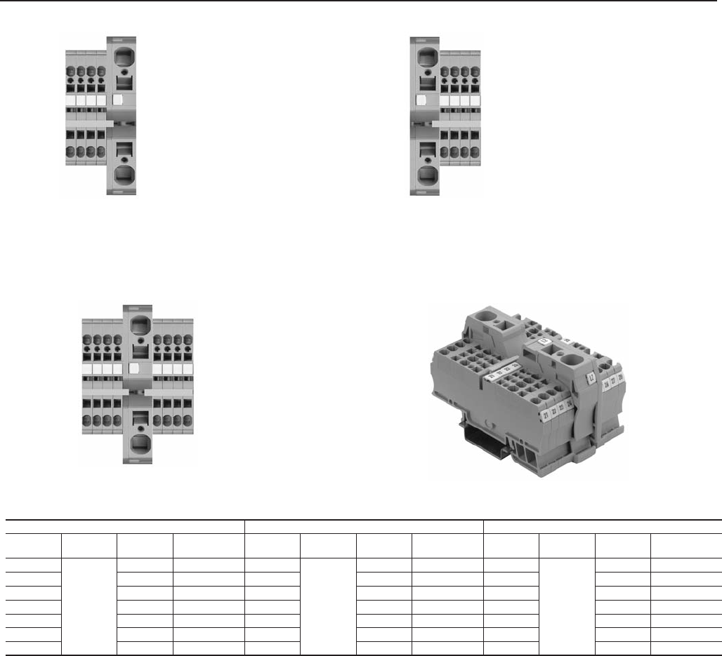
Terminal Block Specifications Spring-Clamp Type Terminal Blocks
29
Rockwell Automation Publication 1492-TD015A-EN-P
Power Distribution Blocks
Feed Left: Feed Right:
The Cat. No. 1492-L16D feed terminal allows wires with a cross section from 4…14 AWG and up to 16 mm
2
to be used. Using standard
cross connections, the potential can be distributed to any number of terminals with smaller cross sections. The following tables show some
variants for potential distribution of the supply, the required cross connection, and the maximum current. The maximum current for the single
terminal block must not be exceeded.
Feed Middle:
Feed Left Feed Middle Feed Right
Feed
Terminal Feed
I
max
Jumper
Feed
Terminal Feed
I
max
Jumper
Feed
Terminal Feed
I
max
Jumper
1492-L3
4…14
AWG
(16 mm
2
)
62 A 1492-CJK5-
1
1492-L3
#4…14
AWG
(16 mm
2
)
76 A 1492-CJK5-
1
1492-L3
#4…14
AWG
(16 mm
2
)
62 A 1492-CJK5-
1
1492-L3Q 62 A 1492-CJK5-
1
1492-L3Q 76 A 1492-CJK5-
1
1492-L3Q 62 A 1492-CJK5-
1
1492-L4 76 A 1492-CJK6-
1
1492-L4 76 A 1492-CJK6-
1
1492-L4 76 A 1492-CJK6-
1
1492-L4T 76 A 1492-CJK6-
1
1492-L4Q 76 A 1492-CJK6-
1
1492-L6 76 A 1492-CJL8-
1
1492-L6 76 A 1492-CJL8-
1
1492-L6 76 A 1492-CJL8-
1
1492-L6T 76 A 1492-CJL8-
1
1
See accessory section for availability of specific jumper pole configurations.

30
Rockwell Automation Publication 1492-TD015A-EN-P
Spring-Clamp Type Terminal Blocks Terminal Block Specifications
1492-LD4 1492-LTF3
Dimensions are not intended to be used
for manufacturing purposes.
Note: Height dimension is measured
from top of rail to top of terminal
block.
0.24"
(6.1 mm)
2.99" (76 mm)
2.06" (52.2 mm)
0.20"
(5.1 mm)
4.35" (110.5 mm)
2.48" (63 mm)
Specifications Two-circuit feed-through terminal block
Three-circuit feed-through terminal block with multiple
cross connection points
Certifications
CSA IEC CSA IEC
Voltage Rating 600V AC/DC 800V AC/DC 300V AC/DC 500V AC/DC
Maximum Current 25 A 30 A 32 A 15 A 20 A
Wire Range (Rated Cross Section) #26…10 AWG
4 mm
2
#26…12 AWG
2.5 mm
2
Wire Strip Length 0.39 in. (10 mm) 0.39 in. (10 mm)
Density 49 pcs/ft (163 pcs/m) 59 pcs/ft (196 pcs/m)
Housing Temperature Range -58…+248 °F (-50…+120 °C) -58…+248 °F (-50…+120 °C)
1492-LD2 1492-LD3 1492-L3QS
Dimensions are not intended to be used
for manufacturing purposes.
Note: Height dimension is measured
from top of rail to top of terminal
block.
0.138"
(3.5 mm)
2.95" (75 mm)
1.69" (43 mm)
0.20"
(5.1 mm)
2.85" (72.5 mm)
1.87" (47.5 mm)
0.20"
(5.1 mm)
3.11" (79 mm)
1.23" (31.3 mm)
Specifications
Two-circuit feed-through
terminal block
Two-circuit feed-through terminal block Side-by-side two circuit terminal block
Certifications
CSA IEC CSA IEC ATEX CSA IEC ATEX
Voltage Rating
300V
AC/DC
600V
AC/DC
500V
AC/DC
600V AC/DC
800V
AC/DC
550V
AC/DC
600V AC/DC
800V
AC/DC
550V
AC/DC
Maximum Current 10 A 17.5 A 20 A 25 A 24 A 20 A 25 A 27 A 24 A 21 A
Wire Range (Rated Cross Section) #28… 16 AWG
1.5 mm
2
#30… 12 AWG
2.5 mm
2
0.5…2.5
mm
2
(#20…14
AWG)
#26… 12 AWG
2.5 mm
2
2.5 mm
2
(20…
12 AWG)
Wire Strip Length 0.39 in. (10 mm) 0.39 in. (10 mm) 0.39 in. (10 mm)
Density 87 pcs/ft (285 pcs/m) 59 pcs/ft (196 pcs/m) 59 pcs/ft (196 pcs/m)
Housing Temperature Range -58…+248 °F (-50…+120 °C) -58…+248 °F (-50…+120 °C) -58…+248 °F (-50…+120 °C)

Terminal Block Specifications Spring-Clamp Type Terminal Blocks
31
Rockwell Automation Publication 1492-TD015A-EN-P
1492-LD2C 1492-LD3C 1492-LD4C
Dimensions are not intended to be used
for manufacturing purposes.
Note: Height dimension is measured
from top of rail to top of terminal
block.
0.138"
(3.5 mm)
2.95" (75 mm)
1.69" (43 mm)
0.20"
(5.1 mm)
2.85" (72.5 mm)
1.87" (47.5 mm)
0.24"
(6.1 mm)
2.99" (76 mm)
2.06" (52.2 mm)
Specifications
Two-level feed-through terminal
block with commoning bar
Two-level feed-through terminal block with
commoning bar
Two-level feed-through terminal
block with commoning bar
Certifications
CSA IEC CSA IEC ATEX CSA IEC
Voltage Rating
300V
AC/DC
600V
AC/DC
500V
AC/DC
600V AC/DC
800V
AC/DC
550V
AC/DC
600V AC/DC
800V
AC/DC
Maximum Current 10 A 17.5 A 20 A 25 A 24 A 22 A 25 A 30 A 32 A
Wire Range (Rated Cross Section) #28…16 AWG 1.5 mm
2
#30…12 AWG 2.5 mm
2
0.5…2.5
mm
2
(#20…14
AWG)
#26…10 AWG 4 mm
2
Wire Strip Length 0.39 in. (10 mm) 0.39 in. (10 mm) 0.39 in. (10 mm)
Density 87 pcs/ft (285 pcs/m) 59 pcs/ft (196 pcs/m) 49 pcs/ft (163 pcs/m)
Housing Temperature Range -58…+248 °F (-50…+120 °C) -58…+248 °F (-50…+120 °C) -58…+248 °F (-50…+120 °C)
1492-LS2-31
1492-LS2-3L1 1492-LSG2-31
1492-LS2-BR
1492-LS2-B
1492-LSG2
Dimensions are not intended to be used
for manufacturing purposes.
Note: Height dimension is measured
from top of rail to top of terminal
block.
0.20"
(5.1 mm)
2.68" (68 mm)
1.52" (38.5 mm)
0.20"
(5.1 mm)
2.68" (68 mm)
1.52" (38.5 mm)
0.20"
(5.1 mm)
0.50" (12.9 mm)
0.69" (17.5 mm)
Specifications
3 conductor sensor block base for
plug in distribution blocks
3 conductor sensor ground block
base for plug in distribution blocks
Plug in Distribution blocks —
internally jumpered
Certifications
CSA IEC CSA IEC CSA IEC
Voltage Rating (without LED) 300V AC/DC
250V
AC/DC
300V AC/DC
250V
AC/DC
300V AC/DC
250V
AC/DC
Voltage Rating (with LED) 5…30V AC/DC — 5…30V AC/DC
Maximum Current 10 A 17.5 A 10 A 17.5 A 10 A 17.5 A
Wire Range (Rated Cross Section) #26…14 AWG 1.5 mm
2
#26…14 AWG 1.5 mm
2
#26…14 AWG 1.5 mm
2
Wire Strip Length 0.31 in. (8 mm) 0.31 in. (8 mm) 0.31 in. (8 mm)
Density 59 pcs/ft (196 pcs/m) 59 pcs/ft (196 pcs/m) 59 pcs/ft (196 pcs/m)
Housing Temperature Range -58…+248 °F (-50…+120 °C) -58…+248 °F (-50…+120 °C) -58…+248 °F (-50…+120 °C)

32
Rockwell Automation Publication 1492-TD015A-EN-P
Spring-Clamp Type Terminal Blocks Terminal Block Specifications
1492-LG2 1492-LG2T 1492-LG2Q
Dimensions are not intended to be used
for manufacturing purposes.
Note: Height dimension is measured
from top of rail to top of terminal
block.
0.138"
(3.5 mm)
2.15" (54.5 mm)
1.16" (29.5 mm)
0.138"
(3.5 mm)
2.48" (63 mm)
1.16" (29.5 mm)
0.138"
(3.5 mm)
2.95" (75 mm)
1.16" (29.5 mm)
Specifications
Feed-through grounding terminal
block
Feed-through grounding terminal
block with 2 points on one side
Feed-through grounding terminal
block with 2 points on each side
Certifications
CSA IEC ATEX CSA IEC ATEX CSA IEC ATEX
Voltage Rating — — — — — — — — — — — —
Maximum Current Grounding Grounding Grounding
Wire Range (Rated Cross Section) #26…14 AWG
1.5
mm
2
1.5 mm
2
(20…
16 AWG)
#26…14 AWG
1.5
mm
2
1.5 mm
2
(20…
16 AWG)
#26…14 AWG
1.5
mm
2
1.5 mm
2
(20…
16 AWG)
Wire Strip Length 0.39 in. (10 mm) 0.39 in. (10 mm) 0.39 in. (10 mm)
Density 87 pcs/ft (285 pcs/m) 87 pcs/ft (285 pcs/m) 87 pcs/ft (285 pcs/m)
Housing Temperature Range -58…+248 °F (-50…+120 °C) -58…+248 °F (-50…+120 °C) -58…+248 °F (-50…+120 °C)
1492-LS2-4
1492-LS2-4L 1492-LSG2-4
1492-LS2-BR
1492-LS2-B
1492-LSG2
Dimensions are not intended to be used
for manufacturing purposes.
Note: Height dimension is measured from
top of rail to top of terminal block.
0.20"
(5.1 mm)
3.19" (81 mm)
1.52" (38.5 mm)
0.20"
(5.1 mm)
3.19" (81 mm)
1.52" (38.5 mm)
0.20"
(5.1 mm)
0.50" (12.9 mm)
0.69" (17.5 mm)
Specifications
4 conductor sensor block base for
plug in distribution blocks
4 conductor sensor ground block
base for plug in distribution blocks
Plug In Distribution blocks —
internally jumpered
Certifications
CSA IEC CSA IEC CSA IEC
Voltage Rating (without LED) 300V AC/DC
250V
AC/DC
300V AC/DC
250V
AC/DC
300V AC/DC
250V
AC/DC
Voltage Rating (with LED) 5…30V AC/DC — 5…30V AC/DC
Maximum Current 10 A 17.5 A 10 A 17.5 A 10 A 17.5 A
Wire Range (Rated Cross Section) #26…14 AWG
1.5 mm
2
#26…14 AWG
1.5 mm
2
#26…14 AWG
1.5 mm
2
Wire Strip Length 0.31 in. (8 mm) 0.31 in. (8 mm) 0.28 in. (7 mm)
Density 59 pcs/ft (196 pcs/m) 59 pcs/ft (196 pcs/m) 59 pcs/ft (196 pcs/m)
Housing Temperature Range -58…+248 °F (-50…+120 °C) -58…+248 °F (-50…+120 °C) -58…+248 °F (-50…+120 °C)

Terminal Block Specifications Spring-Clamp Type Terminal Blocks
33
Rockwell Automation Publication 1492-TD015A-EN-P
1492-LG4 1492-LG4T 1492-LG4Q
Dimensions are not intended to be used
for manufacturing purposes.
Note: Height dimension is measured from
top of rail to top of terminal block.
0.24"
(6.1 mm)
2.44" (62 mm)
1.41" (35.7 mm)
0.24"
(6.1 mm)
3.31" (84 mm)
1.41" (35.7 mm)
0.24"
(6.1 mm)
4.14" (105 mm)
1.41" (35.7 mm)
Specifications
Feed-through grounding terminal
block
Feed-through grounding terminal
block with 2 points on one side
Feed-through grounding terminal
block with 2 points on each side
Certifications
CSA IEC ATEX CSA IEC ATEX CSA IEC ATEX
Voltage Rating — — — — — — — — — — — —
Maximum Current Grounding Grounding Grounding
Wire Range (Rated Cross Section) #26…10 AWG 4 mm
2
4 mm
2
(20…
10 AWG)
#26…10 AWG 4 mm
2
4 mm
2
(20…
12 AWG)
#26…10 AWG 4 mm
2
4 mm
2
(20…
12 AWG)
Wire Strip Length 0.47 in. (12 mm) 0.47 in. (12 mm) 0.47 in. (12 mm)
Density 49 pcs/ft (163 pcs/m) 49 pcs/ft (163 pcs/m) 49 pcs/ft (163 pcs/m)
Housing Temperature Range -58…+248 °F (-50…+120 °C) -58…+248 °F (-50…+120 °C) -58…+248 °F (-50…+120 °C)
1492-LG3 1492-LG3T 1492-LG3Q
Dimensions are not intended to be used
for manufacturing purposes.
Note: Height dimension is measured
from top of rail to top of terminal
block.
0.20"
(5.1 mm)
2.34" (59.5 mm)
1.23" (31.3 mm)
0.20"
(5.1 mm)
2.54" (64.5 mm)
1.23" (31.3 mm)
0.20"
(5.1 mm)
3.11" (79 mm)
1.23" (31.3 mm)
Specifications
Feed-through grounding terminal
block
Feed-through grounding terminal
block with 2 points on one side
Feed-through grounding terminal
block with 2 points on each side
Certifications
CSA IEC ATEX CSA IEC ATEX CSA IEC ATEX
Voltage Rating — — — — — — — — — — — —
Maximum Current Grounding Grounding Grounding
Wire Range (Rated Cross Section)
#30…
12
AWG
#26…
12
AWG
2.5
mm
2
2.5 mm
2
(20…
12 AWG)
#30…
12
AWG
#26…
12
AWG
2.5
mm
2
2.5 mm
2
(20…
12 AWG)
#30…
12
AWG
#26…
12
AWG
2.5
mm
2
2.5 mm
2
(20…
12 AWG)
Wire Strip Length 0.39 in. (10 mm) 0.39 in. (10 mm) 0.39 in. (10 mm)
Density 59 pcs/ft (196 pcs/m) 59 pcs/ft (196 pcs/m) 59 pcs/ft (196 pcs/m)
Housing Temperature Range -58…+248 °F (-50…+120 °C) -58…+248 °F (-50…+120 °C) -58…+248 °F (-50…+120 °C)

34
Rockwell Automation Publication 1492-TD015A-EN-P
Spring-Clamp Type Terminal Blocks Terminal Block Specifications
1492-LG16 1492-LG35 1492-LDG2
Dimensions are not intended to be used
for manufacturing purposes.
Note: Height dimension is measured
from top of rail to top of terminal
block.
0.476"
(12.1 mm)
3.25" (82.5 mm)
1.71" (43.5 mm)
0.634"
(16.1 mm)
3.96" (100.5 mm)
2.04" (51.7 mm)
0.138
(3.5 m
2.95" (75 mm)
Specifications Feed-through grounding terminal block Feed-through grounding terminal block
Two-circuit terminal block with
1 feed-through and 1 ground
circuit
Certifications
CSA IEC ATEX CSA IEC ATEX CSA IEC
Voltage Rating — — — — — — — —
300V
AC/DC
500V
AC/DC
Maximum Current Grounding Grounding 10 A 17.5 A
Wire Range (Rated Cross Section)
#14…6
AWG
#14…4
AWG
16 mm
2
16 mm
2
(16…
6 AWG)
#12…2 AWG
35 mm
2
35 mm
2
(#14…2
AWG)
#28…16 AWG
1.5 mm
2
Wire Strip Length 0.70 in. (18 mm) 0.98 in. (25 mm) 0.31 in. (8 mm)
Density 25 pcs/ft (82 pcs/m) 18 pcs/ft (62 pcs/m) 87 pcs/ft (285 pcs/m)
Housing Temperature Range -58…+248 °F (-50…+120 °C) -58…+248 °F (-50…+120 °C) –58…+248 °F (–50…+120 °C)
1492-LG6 1492-LG6T 1492-LG10
Dimensions are not intended to be used
for manufacturing purposes.
Note: Height dimension is measured
from top of rail to top of terminal
block.
0.319"
(8.1 mm)
2.56" (65 mm)
1.5" (38 mm)
0.319"
(8.1 mm)
3.54" (90 mm)
1.5" (38 mm)
0.398"
(10.1 mm)
2.89" (73.5 mm)
1.67" (42.5 mm)
Specifications
Feed-through grounding terminal
block
Feed-through grounding terminal
block with 2 points on one side
Feed-through grounding terminal
block
Certifications
CSA IEC ATEX CSA IEC ATEX CSA IEC ATEX
Voltage Rating — — — — — — — — — — — —
Maximum Current Grounding Grounding Grounding
Wire Range (Rated Cross Section)
#22…8
AWG
#20…8
AWG
6 mm
2
6 mm
2
(20…
8 AWG)
#22…8
AWG
#20…8
AWG
6 mm
2
6 mm
2
(20…
10 AWG)
#16…6 AWG 10 mm
2
10 mm
2
(16…
8 AWG)
Wire Strip Length 0.51 in. (13 mm) 0.51 in. (13 mm) 0.70 in. (18 mm)
Density 37 pcs/ft (123 pcs/m) 37 pcs/ft (123 pcs/m) 30 pcs/ft (99 pcs/m)
Housing Temperature Range -58…+248 °F (-50…+120 °C) -58…+248 °F (-50…+120 °C) -58…+248 °F (-50…+120 °C)

Terminal Block Specifications Spring-Clamp Type Terminal Blocks
35
Rockwell Automation Publication 1492-TD015A-EN-P
Grounding Blocks
1492-LDG4 1492-LDG4C
Dimensions are not intended to be used
for manufacturing purposes.
Note: Height dimension is measured
from top of rail to top of terminal
block.
0.24"
(6.1 mm)
2.99" (76 mm)
2.06" (52.2 mm)
0.24"
(6.1 mm)
2.99" (76 mm)
2.06" (52.2 mm)
Specifications
Two-circuit grounding terminal block with 1 feed-through
and 1 ground circuit
Single-circuit, two-level grounding terminal block with 2
connection points on each side
Certifications
CSA IEC CSA IEC
Voltage Rating 600V AC/DC 800V AC/DC — — —
Maximum Current 25 A 30 A 32 A Grounding
Wire Range (Rated Cross Section) #26…10 AWG
4 mm
2
#26…10 AWG
4 mm
2
Wire Strip Length 0.39 in. (10 mm) 0.39 in. (10 mm)
Density 49 pcs/ft (163 pcs/m) 49 pcs/ft (163 pcs/m)
Housing Temperature Range -58…+248 °F (-50…+120 °C) -58…+248 °F (-50…+120 °C)
1492-LDG2C 1492-LDG3 1492-LDG3C
Dimensions are not intended to be used
for manufacturing purposes.
Note: Height dimension is measured
from top of rail to top of terminal
block.
0.138"
(3.5 mm)
2.95" (75 mm)
1.69" (43 mm)
0.20"
(5.1 mm)
2.85" (72.5 mm)
1.89" (47.9 mm)
0.20"
(5.1 mm)
2.85" (72.5 mm)
1.89" (47.9 mm)
Specifications
Single-circuit, two-level
grounding terminal block with
2 connection points on each
side
Two-circuit grounding terminal block with
1 feed-through
and 1 ground circuit
Single-circuit, two-level grounding
terminal block with 2 connection points
on each side
Certifications
CSA IEC CSA IEC ATEX CSA IEC ATEX
Voltage Rating — — — 600V AC/DC
800V
AC/DC
550V
AC/DC
————
Maximum Current Grounding 20 A 25 A 24 A 20 A Grounding
Wire Range (Rated Cross Section) #28…16 AWG
1.5 mm
2
#26…12
AWG
#30…12
AWG
2.5 mm
2
0.5…2.5
mm
2
(#20…14
AWG)
#26…12
AWG
#30…12
AWG
2.5 mm
2
0.5…2.5
mm
2
(20…14
AWG)
Wire Strip Length 0.39 in. (10 mm) 0.39 in. (10 mm) 0.39 in. (10 mm)
Density 87 pcs/ft (285 pcs/m) 59 pcs/ft (196 pcs/m) 59 pcs/ft (196 pcs/m)
Housing Temperature Range -58…+248 °F (-50…+120 °C) -58…+248 °F (-50…+120 °C) -58…+248 °F (-50…+120 °C)

36
Rockwell Automation Publication 1492-TD015A-EN-P
Spring-Clamp Type Terminal Blocks Terminal Block Specifications
1492-LKD3
Dimensions are not intended to be used
for manufacturing purposes.
Note: Height dimension is measured
from top of rail to top of terminal
block.
0.20"
(5.1 mm)
2.34" (59.5 mm)
1.29" (32.8 mm)
Specifications Knife disconnect feed-through terminal block
Certifications
CSA IEC
Voltage Rating 600V AC/DC 500V AC/DC
Maximum Current 20 A 24 A
Wire Range (Rated Cross Section) #30…12 AWG
2.5 mm
2
Wire Strip Length 0.39 in. (10 mm)
Density 59 pcs/ft (196 pcs/m)
Housing Temperature Range -58…+248 °F (-50…+120 °C)
1492-LD32P 1492-LG31P 1492-LG3T1P
Dimensions are not intended to be used for
manufacturing purposes.
Note: Height dimension is measured from top of rail to
top of terminal block.
0.20"
(5.1 mm)
3.17" (80.5 mm)
1.77" (45 mm)
0.20"
(5.1 mm)
2.28" (58 mm)
1.08" (27.5 mm)
0.20"
(5.1 mm)
2.82" (71.5 mm)
1.086" (27.5 mm)
Specifications
Two-circuit terminal block with 1
fixed and 1 plug-in connection on
each level. Plug-in connectors can
be individual or grouped
configurations.
Single-circuit grounding terminal
block with 1 fixed and 1 plug-in
connection.
Single-circuit grounding terminal
block with 2 fixed and 1 plug-in
connection.
Certifications
CSA IEC CSA IEC CSA IEC
Voltage Rating 300V AC/DC
500V
AC/DC
————
Maximum Current 20 A 24 A Grounding Grounding
Limited Rating - Voltage
600V AC/DC — — —
Limited Rating - Curr
ent
5 A — — —
Wir
e Range (Rated Cross Section)
26…
12 AWG
0.5…2.5
mm
2
26…
12 AWG
0.5…2.5
mm
2
26…
12 AWG
0.5…2.5
mm
2
Wire Strip Length 0.394 in (10 mm) 0.394 in (10 mm) 0.394 in (10 mm)
Density
(Blocks per
ft/m)
59 pcs/ft (196 pcs/m) 59 pcs/ft (196 pcs/m) 59 pcs/ft (196 pcs/m)
Housing Temperature Range -58…+248 °F (-50…+120 °C) -58…+248 °F (-50…+120 °C) -58…+248 °F (-50…+120 °C)

Terminal Block Specifications Spring-Clamp Type Terminal Blocks
37
Rockwell Automation Publication 1492-TD015A-EN-P
1492-L3P 1492-LDG3P 1492-LDAG3
Dimensions are not intended to be used
for manufacturing purposes.
Note: Height dimension is measured
from top of rail to top of terminal
block.
0.20"
(5.1 mm)
2.34" (59.5 mm)
1.23" (31.3 mm)
0.20"
(5.1 mm)
3.74" (95 mm)
1.61" (41 mm)
0.20"
(5.1 mm)
3.74" (95 mm)
1.61" (41 mm)
Specifications
Single circuit plug-in component
block for a variety of components
Terminal block with slot for plug-in
component, feed-through circuit and
1 ground connection
Analog Loop Control Terminal Block
with 2 Feed-Through Circuits and 1
Ground Connection
Certifications
CSA IEC CSA IEC CSA IEC
Voltage Rating 600V AC/DC
500V
AC/DC
300V AC/DC
250V
AC/DC
300V AC/DC
250V
AC/DC
Maximum Current 20 A 24 A 10 A 20 A 10 A 24 A
Wire Range (Rated Cross Section) #30…12 AWG
4 mm
2
#26…12 AWG
2.5 mm
2
#26…12 AWG
2.5 mm
2
Wire Strip Length 0.39 in. (10 mm) 0.31 in. (8 mm) 0.31 in. (8 mm)
Density 59 pcs/ft (196 pcs/m) 59 pcs/ft (196 pcs/m) 59 pcs/ft (196 pcs/m)
Housing Temperature Range -58…+248 °F (-50…+120 °C) -58…+248 °F (-50…+120 °C) -58…+248 °F (-50…+120 °C)
1492-L31P 1492-L3T1P 1492-L3Q2P
Dimensions are not intended to be used for
manufacturing purposes.
Note: Height dimension is measured from top of rail
to top of terminal block.
0.20"
(5.1 mm)
2.28" (58 mm)
1.08" (27.5 mm)
0.20"
(5.1 mm)
2.82" (71.5 mm)
1.08" (27.5 mm)
0.20"
(5.1 mm)
3.66" (93 mm)
1.08" (27.5 mm)
Specifications
Single circuit terminal block with 1
fixed and 1 plug-in connection.
Plug-in connectors can be
individual or grouped
configurations.
Single circuit terminal block with 2
fixed and 1 plug-in connection.
Plug-in connectors can be
individual or grouped
configurations.
Single circuit terminal block with 2
fixed and 2 plug-in connections.
Plug-in connectors can be
individual or grouped
configurations.
Certifications
CSA IEC CSA IEC CSA IEC
Voltage Rating 300V AC/DC
500V
AC/DC
300V AC/DC
500V
AC/DC
300V AC/DC
500V
AC/DC
Maximum Current 20 A 24 A 20 A 24 A 20 A 24 A
Limited Rating - Voltage‡ 600V AC/DC — 600V AC/DC —
600V
AC/DC
—-
Limited Rating - Curr
ent‡ 5 A—5 A—5 A——
Wir
e Range (Rated Cross Section) #26…12 AWG
0.5...2.5
mm
2
#26…12 AWG
0.5...2.5
mm
2
#26…12 AWG
0.5...2.5
mm
2
Wire Strip Length 0.394 in. (10 mm) 0.394 in. (10 mm) 0.394 in. (10 mm)
Density 59 pcs/ft (196 pcs/m) 59 pcs/ft (196 pcs/m) 59 pcs/ft (196 pcs/m)
Housing Temperature Range –58…+248 °F (–50…+120 °C) –58…+248 °F (–50…+120 °C) –58…+248 °F (–50…+120 °C)

38
Rockwell Automation Publication 1492-TD015A-EN-P
Spring-Clamp Type Terminal Blocks Terminal Block Specifications
1492-LD4DF 1492-LD4DR 1492-LD4SS1
Dimensions are not intended to be used
for manufacturing purposes.
Note: Height dimension is measured
from top of rail to top of terminal
block.
0.24"
(6.1 mm)
2.99" (76 mm)
2.06" (52.2 mm)
0.24"
(6.1 mm)
2.99" (76 mm)
2.06" (52.2 mm)
0.24"
(6.1 mm)
2.99" (76 mm)
2.06" (52.2 mm)
Specifications
Two-level terminal block with an
IN4007 diode in forward bias between
the 2 levels.
Two-level terminal block with an
IN4007 diode in reverse bias between
the 2 levels.
Two level terminal block with an MOV
between the 2 levels.
Certifications
CSA IEC CSA IEC CSA IEC
Voltage Rating 600V AC/DC
500V
AC/DC
600V AC/DC
500V
AC/DC
600V
AC/DC
600V
AC/DC
140V
AC/DC
Maximum Current 25 A 30 A 32 A 25 A 30 A 32 A 120V —
Component Current/Wattage Rating
1
1 A 1 A 25 A 30 A 32 A
Wire Range (Rated Cross Section) #26…10 AWG 4 mm
2
#26…10 AWG 4mm
2
#26…10
AWG
26…10
AWG
4mm
2
Wire Strip Length 0.39 in. (10 mm) 0.39 in. (10 mm) 0.39 in. (10 mm)
Density 49 pcs/ft (163 pcs/m) 49 pcs/ft (163 pcs/m) 49 pcs/ft (163 pcs/m)
Housing Temperature Range -58…+248 °F (-50…+120 °C) -58…+248 °F (-50…+120 °C) –58…+248 °F (–50…+120 °C)
1492-LD32P 1492-LG31P 1492-LG3T1P
Dimensions are not intended to be used
for manufacturing purposes.
Note: Height dimension is measured
from top of rail to top of terminal
block.
0.20"
(5.1 mm)
3.17" (80.5 mm)
1.77" (45 mm)
0.20"
(5.1 mm)
2.28" (58 mm)
1.08" (27.5 mm)
0.20"
(5.1 mm)
2.82" (71.5 mm)
1.086" (27.5 mm)
Specifications
Two- circuit terminal block with 1 fixed
and 1 plug-in connection. Plug-in
connectors can be individual or
grouped configurations.
Single circuit grounding terminal block
with 1 fixed and 1 plug-in connection.
Single circuit grounding terminal block
with 2 fixed and 1 plug-in connection.
Certifications
CSA IEC CSA IEC CSA IEC
Voltage Rating 300V AC/DC
500V
AC/DC
——
Maximum Current 20 A 24 A Grounding Grounding
Limited Rating - Voltage
600V AC/DC — — —
Limited Rating - Curr
ent
5 A — — —
Wir
e Range (Rated Cross Section) #26…12 AWG
0.5...2.5
mm
2
#26…12 AWG
0.5...2.5
mm
2
#26…12 AWG
0.5...2.5
mm
2
Wire Strip Length 0.394 in. (10 mm) 0.394 in. (10 mm) 0.394 in. (10 mm)
Density 59 pcs/ft (196 pcs/m) 59 pcs/ft (196 pcs/m) 59 pcs/ft (196 pcs/m)
Housing Temperature Range –58…+248 °F (–50…+120 °C) –58…+248 °F (–50…+120 °C) –58…+248 °F (–50…+120 °C)
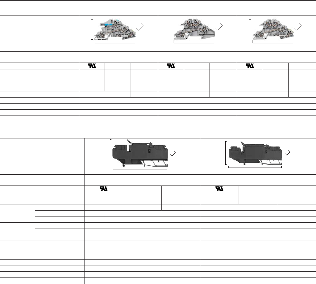
Terminal Block Specifications Spring-Clamp Type Terminal Blocks
39
Rockwell Automation Publication 1492-TD015A-EN-P
1492-RFB4… 1492-RAFB4…
Dimensions are not intended to be used
for manufacturing purposes.
Note: Height dimension is measured
from top of rail to top of terminal
block.
0.31"
(8 mm)
3.82" (97 mm)
1.72" (43.8 mm)
0.39"
(10 mm)
4.33" (110 mm)
1.76" (44.8 mm)
Specifications
Single-circuit fuse terminal block with or without blown
fuse indicator
Single-circuit fuse terminal block with or without blown
fuse indicator
Certifications
cUR IEC cUR IEC
Maximum Current 15 A
1 15 A1 15 A1
12 A 12 A 12 A
Wire Range (Rated Cross Section) #22…12 AWG #22…12 AWG 0.5…4 mm
2
#22…12 AWG #22…12 AWG 0.5…4 mm
2
Voltage Rating
RFB4/RAFB4 300V AC/DC 500V AC/DC 300V AC/DC 500V AC/DC
RFB424/RAFB424 10…57V AC/DC 10…57V AC/DC
RFB4250/RAFB4250 85…264V AC 85…264V AC
Indicator Type
RFB4/RAFB4 Non-indicating Non-indicating
RFB424/RAFB424 LED LED
RFB4250/RAFB4250 LED LED
Leakage Current
RFB4/RAFB4 — —
RFB424/RAFB424 2 mA @ 24V 2 mA @ 24V
RFB4250/RAFB4250 1 mA @ 264V 1 mA @ 264V
Fuse Size (Not Supplied) 5 x 20 mm 1/4 x 1 -1/4 in.
Wire Strip Length 0.47 in. (12 mm) 0.47 in. (12 mm)
Density 37 pcs/ft (125 pcs/m) 30 pcs/ft (100 pcs/m)
Insulation Temperature Range -4…+140 °F (-20…+60 °C) -4…+221 °F (-40…+105 °C)
1492-LDG3ND 1492-LD3N 1492-LDG3N
Dimensions are not intended to be
used for manufacturing purposes.
Note: Height dimension is measured
from top of rail to top of terminal
block.
3.74” (95 mm)
0.201”
(5.1 mm)
1.61” (41 mm)
3.74” (95 mm)
0.201”
(5.1 mm)
1.61” (41 mm)
3.74” (95 mm)
0.201”
(5.1 mm)
1.61” (41 mm)
Specifications
3-Level terminal block with neutral
disconnect and ground connection
2-Level feed-through terminal block for
installation applications
3-Level terminal block with 2 feed-
through and ground connection
Certifications
CSA IEC CSA IEC CSA IEC
Voltage Rating
600V
AC/DC
300V
AC/DC
400V AC/DC
600V
AC/DC
300V
AC/DC
400V AC/DC
600V
AC/DC
300V
AC/DC
400V AC/DC
Maximum Current 15 A 10 A 24 A
15 A
10 A 24 A 15 A 10 A 24 A
Wire Range (Rated Cross Section) #26…12 AWG 2.5 mm
2
#26…12 AWG 2.5 mm
2
#26…12 AWG 2.5 mm
2
Wire Strip Length 0.31 in. (8 mm) 0.31 in. (8 mm) 0.31 in. (8 mm)
Density 59 pcs/ft (196 pcs/m) 59 pcs/ft (196 pcs/m) 59 per ft/196 per meter
Housing Temperature Range -58...+248 °F (-50...+120 °C) -58...+248 °F (-50...+120 °C) -58...+248°F (-50...+120°C)

40
Rockwell Automation Publication 1492-TD015A-EN-P
Spring-Clamp Type Terminal Blocks Terminal Block Specifications
1492-LC3 1492-LDC3
Dimensions are not intended to be used for
manufacturing purposes.
Note: Height dimension is measured from
top of rail to top of terminal block.
0.20"
(5.1 mm)
1.81" (46 mm)
1.06" (26.9 mm)
0.20"
(5.1 mm)
2.72" (69 mm)
1.67" (42.5 mm)
Specifications
Feed-through terminal block with plug in comb
connection on one side.
Two Circuit terminal block with plug in comb connection
on one side of each circuit
Certifications
CSA IEC CSA IEC
Voltage Rating 300V AC/DC 250V AC/DC 300V AC/DC 250V AC/DC
Maximum Current 10 A 16 A 10 A 16 A
Wire Range (Rated Cross Section) #26…12 AWG
2.5 mm
2
#26…14 AWG
2.5 mm
2
Wire Strip Length 0.39 in. (10 mm) 0.39 in. (10 mm)
Density 59 pcs/ft (196 pcs/m) 59 pcs/ft (196 pcs/m)
Housing Temperature Range -58…+248 °F (-50…+120 °C) -58…+248 °F (-50…+120 °C)
1492-LAFB6
Dimensions are not intended to be used for manufacturing purposes.
Note: Height dimension is measured from top of rail to top of terminal
block.
0.319"
(8.1 mm)
2.76" (70 mm)
1.85" (47 mm)
Specifications
Single-circuit automotive style fuse terminal block with or without LED blown fuse
indication
Certifications
CSA IEC
Voltage Rating
-LAFB6 300V AC/DC 250V AC/DC
-LAFB624 10…36V AC/DC
Maximum Current 30 A 25 A 30 A
Wire Range (Rated Cross Section) #22…12 AWG
#22…
10 AWG
0.5…6 mm
2
Wire Strip Length 0.394 in. (10 mm)
Density 37 pecs/ft (123 pcs/m)
Housing Temperature Range -58…+248 °F (-50…+120 °C)
Plug-in Connection Blocks

Terminal Block Specifications Spring-Clamp Type Terminal Blocks
41
Rockwell Automation Publication 1492-TD015A-EN-P
Cat. No.
Wire Cu [AWG] Overcurrent Protection Fuse Required Class/Max. Amp Rating
Maximum
Voltage
SCCR, RMS
SYM [A]Line Load J T RK1 RK5 G CC
1492-L3
14…12 14…12 30
30 — — 30 30 600 100,000
1492-L3Q
1492-L3T
1492-LD3
1492-L3QS
1492-LMJ3
1492-LMJG3
1492-LKD3
1492-L3P
1492-LG3T
1492-LG3Q
1492-LG3
1492-LD3C
1492-LDG3C
1492-LDG3
1492-LC3
14…12 14…12 30
30 — — 30 30 300 100,000
1492-LDC3
1492-LDG3P
1492-LDG3ND
1492-LDG3N
1492-LD3N
1492-LD31P
1492-LD3Q2P
1492-LG31P
1492-LG3T1P
1492-L3T1P
1492-LDG3FB
1492-L4
14…10 14…10 60
60 30 — 30 30 600 100,000
1492-L4Q
1492-L4T
1492-LD4
1492-LD4C
1492-LG4
1492-LG4T
1492-LG4Q
1492-LD4DFX2
1492-L6
14…8 14…8 60
60 30 — 60 30 600 100,000
1492-L6T
1492-LG6
1492-LG6T
1492-LAFB6 14…8 14…8 60 60 30 — 60 30 300 100,000
1492-L10
14…6 14…6 100
100 60 30 60 30 600 100,000
1492-LG10
1492-L16
14…4 14…4 100
100 60 30 60 30 600 100,000
1492-LG16
1492-L35
12…2 12…2 200
200 100 30 60 30 600 100,000
1492-LG35
Short-Circuit Current Ratings — Fuse Ratings

42
Rockwell Automation Publication 1492-TD015A-EN-P
IEC Terminal Block Accessories Terminal Block Specifications
Mounting Rails
Cat. No. Description Pkg Qty.
Dimensions
199-DR1
Symmetrical Rail
35 mm x 7.5 mm
3.28 ft (1 m) long
Zinc-Plated Clear
Chromated Steel
EN60715
DIN #3
10
199-DR2
Same as Cat. No. 199-DR1,
but length = 2 m
20
199-DR4
Heavy Duty
Symmetrical Rail
35 mm x 15 mm
3.28 ft (1 m) long
Zinc-Plated Clear
Chromated Steel
EN60715
DIN #3
5
1492-DR3
Mini 15 mm x 5.5 mm
Rail 3.28 ft (1 m) long
Zinc-Plated Clear
Chromated Steel
EN60715
DIN #2
5
1492-DR5
Symmetrical Rail
35 mm x 7.5 mm
3.28 ft (1 m) long
Copper-Free
Aluminum EN60715
For Bul. 1492 Terminal Blocks
Only
DIN #3
10
‡
1492-DR6
Symmetrical Rail
35 mm x 7.5 mm
2.26 in. (57.4 mm) high
3.28 ft (1 m) long
Copper-Free
Aluminum
For Bul. 1492 Terminal Blocks
Only
DIN #3
2
‡
1492-DR7
Symmetrical Rail
35 mm x 7.5 mm
2.80 in. (71.0 mm) high
3.28 ft (1 m) long
Angled 30°
Zinc-Plated,
Chromated Steel
DIN #3
2
1492-DR8
Symmetrical Rail
35 mm x 15 mm
3.28 ft (1 m) long
Copper
EN60715
DIN #3
5
§
1492-DR9
Symmetrical Rail
35 mm x 15 mm
3.28 ft (1 m) long
Zinc-Plated Clear
Chromated Steel
EN60715
DIN #3
5
2.5
0.3
0.2
15±
15°±1°
0.2
0.04
Detail A
See Detail A
24±0.3
35±0.3
25±0.3
5.2±0.2
18±0.3
Dimensions shown in inches (millimeters). Dimensions are not intended to be used for manufacturing purposes.
‡ 0.218 x 0.50 in. (5.5 x 12.7 mm) slotted mounting holes every 3 in. (76.2 mm) starting 1.69 in. (42.9 mm) from end.
§ Dimensions in millimeters.

43
Rockwell Automation Publication 1492-TD015A-EN-P
Terminal Block Specifications IEC Terminal Block Accessories
End Barriers
Dimensions
Width x Length x Height For Use With Color
Pkg
Qty.
Cat. No.
0.08 x 1.14 x 2.03 in.
(2 x 28.9 x 51.5 mm)
1492-L2, LG2
Grey 50
1492-EBL2
Blue 50
1492-EBL2-B
Yellow 50
1492-EBL2-Y
0.08 x 1.14 x 2.48 in.
(2 x 28.9 x 63 mm)
1492-L2T, LG2T
Grey 50
1492-EBL2T
Blue 50 1492-EBL2T-B
Yellow 50
1492-EBL2T-Y
0.08 x 1.14 x 2.95 in.
(2 x 28.9 x 75 mm)
1492-L2Q, LG2Q
Grey 50
1492-EBL2Q
Blue 50
1492-EBL2Q-B
Yellow 50 1492-EBL2Q-Y
0.08 x 1.15 x 2.34 in.
(2 x 29.1 x 59.5 mm)
1492-L3, LG3, LKD3, L3P
Grey 50
1492-EBL3
Blue 50
1492-EBL3-B
Yellow 50
1492-EBL3-Y
0.08 x 1.20 x 2.54 in.
(2 x 30.6 x 64.5 mm)
1492-L3T, LG3T
Grey 50
1492-EBL3T
Blue 50
1492-EBL3T-B
Yellow 50
1492-EBL3T-Y
0.08 x 1.20 x 3.11 in.
(2 x 30.6 x 79 mm)
1492-L3Q, L3QS, LG3Q
Grey 50
1492-EBL3Q
Blue 50
1492-EBL3Q-B
Yellow 50
1492-EBL3Q-Y
0.10 x 1.06 x 2.8 in.
(2.5 x 27 x 71 mm)
1492-L31P, 1492-LG31P Yellow 50
1492-EBL31P-Y
1492-L3T1P, 1492-LG3T1P
Grey 50
1492-EBL3T1P
Yellow 50
1492-EBL3T1P-Y
0.08 x 1.20 x 3.11 in.
(2 x 30.6 x 79 mm)
1492-L3Q2P Grey 50
1492-EBL3Q2P
0.10 x 1.76 x 3.17 in.
(2.5 X 44.7 x 80.5)
1492-LD32P Grey 50
1492-EBLD32P
0.08 x 1.37 x 2.44 in.
(2 x 34.85 x 62 mm)
1492-L4, LG4
Grey 50
1492-EBL4
Blue 50
1492-EBL4-B
Yellow 50
1492-EBL4-Y
0.08 x 1.37 x 3.31 in.
(2 x 34.85 x 84 mm)
1492-L4T, LG4T
Grey 50
1492-EBL4T
Blue 50 1492-EBL4T-B
Yellow 50
1492-EBL4T-Y
0.08 x 1.37 x 4.13 in.
(2 x 34.85 x 105 mm)
1492-L4Q, LG4Q
Grey 50
1492-EBL4Q
Blue 50 1492-EBL4Q-B
Yellow 50
1492-EBL4Q-Y
0.08 x 1.45 x 2.56 in.
(2 x 36.95 x 65 mm)
1492-L6, LG6
Grey 50
1492-EBL6
Blue 50 1492-EBL6-B
Yellow 50
1492-EBL6-Y
0.08 x 1.45 x 3.54 in.
(2 x 36.95 x 90 mm)
1492-L6T, LG6T
Grey 50
1492-EBL6T
Blue 50 1492-EBL6T-B
Yellow 50
1492-EBL6T-Y
0.12 x 1.67 x 2.89 in.
(3 x 42.5 x 73.5 mm)
1492-L10, LG10
Grey 20
1492-EBL10
Blue 20 1492-EBL10-B
Yellow 20
1492-EBL10-Y
0.12 x 1.71 x 3.25 in.
(3 x 43.5 x 82.5 mm)
1492-L16, LG16
Grey 20
1492-EBL16
Blue 20 1492-EBL16-B
Yellow 20
1492-EBL16-Y
— 1492-LAFB6 Black 50
1492-EBLAFB6
0.08 x 1.65 x 2.95 in.
(2 x 41.9 x 75 mm)
1492-LD2, LDG2, LD2C, LDG2C
Grey 50
1492-EBLD2
Blue 20 1492-EBLD2-B
Yellow 20
1492-EBLD2-Y
0.08 x 1.87 x 2.85 in.
(2 x 47.5 x 72.5 mm)
1492-LD3, LD3C, LDG3, LDG3C
Grey 20
1492-EBLD3
Blue 20 1492-EBLD3-B
Yellow 20
1492-EBLD3-Y
0.08 x 2.05 x 2.99 in.
(2 x 52 x 76 mm)
1492-LD4, LD4C, LDG4, LDG4C, LD4DF, LD4DR, LD4RB…,
LD4SS
Grey 20
1492-EBLD4
Blue 20
1492-EBLD4-B
Yellow 20 1492-EBLD4-Y
End barriers are required to provide the necessary insulation for the last terminal block in a group.

44
Rockwell Automation Publication 1492-TD015A-EN-P
IEC Terminal Block Accessories Terminal Block Specifications
End Barriers
Photo
Dimensions
Width x Length x Height
Tightening
Torque Markers For Use With Color Pkg Qty. Cat. No.
0.31 x 2.20 x 1.85 in.
(8 x 56 x 47 mm)
4.4 lb•in
(0.5 N•m)
1492-M7X12
1492-M8X5
199-DR1, 199-DR2,
1492-DR4, 1492-DR5,
1492-DR6, 1492-DR7,
1492-DR8, 1492-DR9
Grey 100
1492-EAJ35
0.48 x 2.20 x 2.48 in.
(12.2 x 56 x 63 mm)
4.4 lb•in
(0.5 N•m)
1492-M7X12
1492-M5X5
199-DR1, 199-DR2,
1492-DR4, 1492-DR5,
1492-DR6, 1492-DR7,
1492-DR8, 1492-DR9
Grey 50
1492-EAHJ35
0.31 x 1.06 x 1.06 in.
(8 x 27 x 27 mm)
3.5 lb•in
(0.9 N•m)
1492-M5X5 1492-DR3 Grey 50
1492-EAJ15
0.24 x 2.19 x 1.63 in.
(6 x 55.6 x 41.5 mm)
—
1492-M5X10
1492-M5X5
199-DR1, 199-DR2,
1492-DR4, 1492-DR5,
1492-DR6, 1492-DR7,
1492-DR8, 1492-DR9
Grey 20
1492-ERL35
0.20 x 0.96 x 0.75 in.
(5 x 24.5 x 19 mm)
—
1492-M5X10
1492-M5X5
1492-DR3 Grey 20
1492-ERL15
Dimensions
Width x Length x Height For Use With Color Pkg Qty.
Cat. No.
0.20 x 0.94 x 1.31 in.
(5.1 x 23.8 x 33.3 mm)
1492-LMP3, LMP3Q
Grey 50
1492-EBLMP3
Blue 50 1492-EBLMP3-B
0.20 x 0.94 x 1.31 in.
(5.1 x 23.8 x 33.3 mm)
1492-LM3, LM3Q, LMG3,
LMP3E, LMP3QE
Grey 50
1492-EBLM3
0.06 x 0.97 x 1.38 in.
(1.5 x 24.65 x 35 mm)
1492-LMJ3, LMJG3
Grey 50
1492-EBLMJ3
Blue 50 1492-EBLMJ3-B
Yellow 50
1492-EBLMJ3-Y
0.06 x 2.32 x 4.35 in.
(1.5 x 59 x 110.5 mm)
1492-LTF3
Grey
20
1492-EBLTF3
0.06 x 2.69 x 1.77 in.
(5 x 68.5 x 45 mm)
1492-LS2-3, LS2-3L, LSG2-3 50
1492-EBLS2-3
0.20 x 3.2 x 1.77 in.
(5 x 81.5 x 45 mm)
1492-LS2-4, LS2-4L, LSG2-4 50
1492-EBLS2-4
0.06 x 1.81 x 3.74 in.
(1.5 x 46 x 95 mm)
1492-LDAG3, LDG3P 20
1492-EBLDAG3
0.10 x 1.04 x 1.81 in.
(2.5 x 26.4 x 46 mm)
1492-LC3 20
1492-EBLC3
0.10 x 1.65 x 2.72 in.
(2.5 x 41.85 x 69 mm)
1492-LDC3 20
1492-EBLDC3
— 1492-LDG3ND, LD3N, LDG3N Grey 20
1492-BSPJLD3N
— 1492-LDG3ND, LD3N, LDG3N Blue 20 1492-BSPJLD3N-B
End Anchor/End Retainers
End anchors and end retainers mount at both ends of a group of terminal blocks to add rigidity to the terminal assembly and prevent sliding
along the rails.

45
Rockwell Automation Publication 1492-TD015A-EN-P
Terminal Block Specifications IEC Terminal Block Accessories
Partition plates allow visual and electrical separation of terminal groups and provide the necessary electrical spacing between adjacent
insulated jumpers or between exposed ends of cut jumpers.
Separation plates consist of flexible thermoplastic material and are used between terminal blocks to isolate adjacent center jumpers both
visually and electrically.
Dimensions
Width x Length x Height For Use With Color
Pkg
Qty.
Cat. No.
Partition Plates
0.118 x 3.15 x 2.48 in.
(3 x 80 x 63 mm)
1492-JD3, JD3C, JD3F, JD3DF, JD3DR, JD3RC…, JD3SS Grey 20
1492-PPJD3
0.005 x 3.54 x 2.51 in.
(0.13 x 90.1 x 63.8 mm)
1492-JD3P…, JDG3P… Beige 20
1492-PPJD3P
0.08 x 1.57 x 1.20 in.
(2 x 40 x 30.5 mm)
1492-WM3, WM4, WMG3, WMG4 Grey 50
1492-PPM3
0.014 x 2.28 x 1.51 in.
(0.35 x 58 x 38.3 mm)
1492-WMD1 Grey 50
1492-PPMD1
0.06 x 1.85 x 1.57 in.
(1.5 x 47 x 40 mm)
1492-W3, W4, WG4 Grey 50
1492-PP3
0.06 x 2.17 x 1.81 in.
(1.5 x 55 x 46 mm)
1492-W6, W10, W16S, W4TW, WG6, WG10S, WG16S Grey 50
1492-PP10
0.014 x 2.88 x 1.85 in.
(0.35 x 73.2 x 47.1 mm)
1492-WTF3…, WTS3… Beige 50
1492-PPTS3
0.06 x 1.93 x 2.36 in.
(1.5 x 49 x 60 mm)
1492-J3, J4, J6, J10, J2Q, J3TW, J3F, JG2Q, JG3, JG3TW,
JKD3, JKD3TP, J3P, J3PTP, JTC3
Grey 20
1492-EBJ16
Blue 20
1492-EBJ16-B
Yellow 20
1492-EBJ16-Y
Separation Plates
.014 x 1.76 x 1.57 in.
(0.35 x 44.8 x 40.0 mm)
1492-W3, W4 Beige 50
1492-SP3
All 1492-FPK2 Fuse Plugs Beige 50
1492-SPJ3
Partition Plates and Separation Plates

46
Rockwell Automation Publication 1492-TD015A-EN-P
IEC Terminal Block Accessories Terminal Block Specifications
Photo For Use With Color
Pkg
Qty. Cat. No.
Center Jumper Spacer Plate
1492-L4 to 1492-L3Q, L3
1492-L6 to 1492-L3Q, L3
Grey 25
1492-LJS
Photo For Use With
Pkg
Qty. Cat. No.
1492-J35 to 1492-J4 or J6 10
1492-CJJ16SD68
1492-J16 to 1492-J4 or J6 10
1492-CJJ12SD68
1492-J35 to 1492-J3 10 1492-CJJ16SD5
1492-J16 to 1492-J3 10
1492-CJJ12SD5
Step-Down Distribution Jumpers
Center Jumper Configuration Plates
Center jumper covers can be used as an extruded marking surface for circuit identification.
Center Jumper Covers
These center jumpers are insulated and are available in 2-…50-pole configurations. They mount without screws into the both Spring-Clamp
terminal blocks and some screw terminal blocks.
Note: When using multiple screwless jumpers in 1492-J3, 1492-J2Q, or 1492-J4 terminal blocks, the following rules apply when going
across different potentials with jumpers cut out:
When using all 3 channels, or 2 side-by-side channels, de-rate to 125V
When using 2 outside channels (leaving the center channel open), de-rate to 400V
Always use a partition plate where a cut jumper strip may leave a live end exposed
Center Jumpers — Screwless Type
These center jumpers are insulated and are available in 2-…50-pole configurations. They mount with screws into the screw type terminal
blocks.
Note: The following rules apply when going across different potentials with jumpers cut out:
Always de-rate to 400V
Always use a partition plate where a cut jumper strip may leave a live end exposed
Center Jumpers — Screw Type
Jumpers use the terminal block wire openings. Multi-pole jumpers can be cut into a smaller number of poles. Jumpers carry 100% of rated
terminal block current. The back of IEC style jumpers are insulated with plastic. An adjacent partition plate provides the necessary electrical
spacings between adjacent jumpers or between exposed ends of cut jumpers.

47
Rockwell Automation Publication 1492-TD015A-EN-P
Terminal Block Specifications IEC Terminal Block Accessories
For Use With
For Use With
Pkg
Qty.
Cat. No.
1492-J3, JD3…, JDG3…,
J2Q, J3TW, J3F, JD3F
50
1492-CJJ5-2
50
1492-CJJ5-3
50
1492-CJJ5-4
20
1492-CJJ5-10
1492-J4, J4M
50
1492-CJJ6-2
50
1492-CJJ6-3
50
1492-CJJ6-4
20
1492-CJJ6-10
1492-J6
50
1492-CJJ8-2
50
1492-CJJ8-3
50
1492-CJJ8-4
20
1492-CJJ8-10
1492-J10
50
1492-CJJ10-2
50
1492-CJJ10-3
50
1492-CJJ10-4
20
1492-CJJ10-10
1492-J16
20
1492-CJJ12-2
20
1492-CJJ12-3
20
1492-CJJ12-4
10
1492-CJJ12-10
1492-J35
20
1492-CJJ16-2
20
1492-CJJ16-3
20 1492-CJJ16-4
10
1492-CJJ16-10
1492-J50
10
1492-CJJ18-2
10 1492-CJJ18-3
10
1492-CJJ18-4
1492-J70
5
1492-CJJ20-2
5
1492-CJJ20-3
5
1492-CJJ20-4
1492-WM3
10
1492-CJM5-2
10
1492-CJM5-3
10 1492-CJM5-4
10
1492-CJM5-5
10
1492-CJM5-10
1492-W3, WM3, WR3,
WTF3…, WTS3…
10
1492-CJL5 (Link)
1492-WR3
5
1492-CJD5-50
10
1492-CJD5-2
10
1492-CJD5-3
10 1492-CJD5-4
10
1492-CJD5-5
10
1492-CJD5-10
Note: Notching out one or more jumper poles, with the notched jumpers
going across different potentials, will require de-rating to 400V.
Pkg
Qty.
Cat. No.
1492-WM4
5
1492-CJD6-50
10
1492-CJD6-2
10
1492-CJD6-3
10 1492-CJD6-4
10
1492-CJD6-5
10
1492-CJD6-10
1492-WM4, W4TW 10 1492-CJLD6 (Link)
1492-W3
10
1492-CJ5-2
10
1492-CJ5-3
10
1492-CJ5-10
20
1492-CJCW5
(CJ Cover)
1492-WTF3…, WTS3…
5
1492-CJT5-50
10
1492-CJT5-2
10 1492-CJT5-3
10
1492-CJT5-4
10
1492-CJT5-5
10
1492-CJT5-10
1492-W4, W4TW
5
1492-CJ6-50
10
1492-CJ6-2
10
1492-CJ6-3
10
1492-CJ6-4
10
1492-CJ6-5
10
1492-CJ6-10
1492-W4 10 1492-CJL6 (Link)
1492-W4, W6, W10 20
1492-CJCW6
(CJ Cover)
1492-W6
5
1492-CJ7-40
10
1492-CJ7-2
10
1492-CJ7-3
10
1492-CJ7-4
10 1492-CJ7-5
10
1492-CJ7-10
1492-W6 10 1492-CJL7 (Link)
1492-W10
5
1492-CJ8-40
10
1492-CJ8-2
10
1492-CJ8-3
10 1492-CJ8-4
10
1492-CJ8-5
10
1492-CJ8-10
1492-W10 10 1492-CJL8 (Link)
1492-W16S
10
1492-CJS11-2
10
1492-CJS11-3
10 1492-CJS11-4
10
1492-CJS11-5
10
1492-CJS11-10
May only be used as a marking surface. May not be installed over center
jumper.
Screw Type Center Jumpers

48
Rockwell Automation Publication 1492-TD015A-EN-P
IEC Terminal Block Accessories Terminal Block Specifications
For Use With Color Pkg Qty. Cat. No.
1492-L2…, L2T,
L2Q, LD2, LD2C
Yellow
60
1492-CJL4-2
60
1492-CJL4-3
60
1492-CJL4-4
60
1492-CJL4-5
20
1492-CJL4-10
1492-LM3, LC3,
LDC3,
LDAG3, LDG3P,
JKD3…,
J3P…, J3, J3TW (see
Note)
Yellow 60
1492-CJLJ5-2
Black 60 1492-CJLJ5-2-BL
Yellow 60
1492-CJLJ5-3
Yellow
60
1492-CJLJ5-4
20
1492-CJLJ5-5
20
1492-CJLJ5-6
20
1492-CJLJ5-7
20
1492-CJLJ5-8
20 1492-CJLJ5-9
20
1492-CJLJ5-10
Red 20
1492-CJLJ5-10-R
Black 20
1492-CJLJ5-10-BL
Yellow 10
1492-CJLJ5-50
Red 10
1492-CJLJ5-50-R
Blue 10 1492-CJLJ5-50-B
Black 10
1492-CJLJ5-50-BL
White 10
1492-CJLJ5-50-W
For Use With Pkg Qty. Cat. No.
1492-RFB4
10
1492-CJR8-2
10
1492-CJR8-3
10
1492-CJR8-4
10
1492-CJR8-5
10
1492-CJR8-6
10
1492-CJR8-7
10
1492-CJR8-8
10
1492-CJR8-9
10
1492-CJR8-10
1492-RAFB4
10
1492-CJRA10-2
10
1492-CJRA10-3
10
1492-CJRA10-4
10
1492-CJRA10-5
For Use With Color Pkg Qty. Cat. No.
1492-J4, J4M (see
Note)
Yellow 60
1492-CJLJ6-2
Red 60 1492-CJLJ6-2-R
Blue 60
1492-CJLJ6-2-B
Black 60
1492-CJLJ6-2-BL
Yellow 60
1492-CJLJ6-3
Blue 60 1492-CJLJ6-3-B
Black 60
1492-CJLJ6-3-BL
Yellow 60
1492-CJLJ6-4
Yellow 20
1492-CJLJ6-10
Red 20
1492-CJLJ6-10-R
Blue 20
1492-CJLJ6-10-B
Black 20
1492-CJLJ6-10-BL
Yellow 10
1492-CJLJ6-41
Red 10
1492-CJLJ6-41-R
Blue 10 1492-CJLJ6-41-B
Black 10
1492-CJLJ6-41-BL
1492-L6, L6T, L16D Yellow
60
1492-CJL8-2
60
1492-CJL8-3
60
1492-CJL8-4
10
1492-CJL8-32
1492-L10 Yellow 25
1492-CJL10-2
1492-L16 Yellow 25
1492-CJL12-2
1492-L35 Yellow 10
1492-CJL16-2
1492-L3, L3T, L3Q,
L3P,
LD3, LD3C, LKD3,
LTF3,
LS2…, L16D
Yellow
60
1492-CJK5-2
60
1492-CJK5-3
60
1492-CJK5-4
20
1492-CJK5-5
20
1492-CJK5-6
20
1492-CJK5-7
20
1492-CJK5-8
20
1492-CJK5-9
20
1492-CJK5-10
10
1492-CJK5-50
1492-L4, L4T, L4Q,
LD4DF,
LD4DR, LD4SS,
LD4, LD4C, L16D
Yellow
60
1492-CJK6-2
60
1492-CJK6-3
60
1492-CJK6-4
20
1492-CJK6-5
20
1492-CJK6-6
20 1492-CJK6-7
20
1492-CJK6-8
20 1492-CJK6-9
20
1492-CJK6-10
20
1492-CJK6-20
Screwless Center Jumpers

49
Rockwell Automation Publication 1492-TD015A-EN-P
Terminal Block Specifications IEC Terminal Block Accessories
For Use With
Pkg
Qty. Cat. No.
1492-WM4, W4 50
1492-N42
1492-H4, H5, H6, H7
10
1492-N49
For Use With
Pkg
Qty. Cat. No.
1492-LTF3
(Connects Two Levels within a 1492-LTF3
Terminal Block)
20
1492-CJL5D
10
1492-SJS
1492-W3, WR3 10
1492-SJ5-10
1492-JD3, JD3C, JD3F, JDG3, JD3DF,
JD3DR, JD3SS, JDG3P
50
1492-SJ5A-10
1492-JD3, JD3C, JD3F, JDG3, JD3DF,
JD3DR, JD3SS, JDG3P
50
1492-SJ5A-24
1492-JD3, JD3C, JD3F, JDG3, JD3DF,
JD3DR, JD3SS, JDG3P
50
1492-SJ5B-24
1492-JD3, JD3C, JD3F, JDG3, JD3DF,
JD3DR, JD3SS, JDG3P
50
1492-SJ5B-10
1492-WM4, W4, W4TW 10 ‡
1492-SJ6-10
1492-JT3M 5
1492-SJ6A-50
1492-W10 10
1492-SJ8-10
1492-JD3FB, JDG3FB 50
1492-SJ8A-4
1492-JD3FB, JDG3FB 50 1492-SJ8A-3
1492-JD3FB, JDG3FB 50
1492-SJ8A-2
1492-LMP3, LMP3Q, LMJ3, LM3, LM3Q,
LMP3E, LMP3QE
50
1492-SJLM5-2
1492-WMD1 10 §
1492-SJMD5-12
1492-WFB4, WFB424, WFB4250 10
1492-SJFB8-10
1492-WM3 10
1492-SJM5-10
1492-WTF3, WTS3, WTF3LP, WTS3LP,
WTF3LP, WTF3LN, WTS3LN
10
1492-SJT5-20-R
1492-WTF3, WTS3, WTF3LP, WTS3LP,
WTF3LP, WTF3LN, WTS3LN
10
1492-SJT5-20-B
Note: Side jumpers carry the same current rating as the terminal block used
with it
Side jumper insulating sleeve only for use with Cat. No. 1492-N49
‡ Use jumper on single side of terminal block only
§ Uninsulated
Two-Level Jumper
Side Jumpers

Sockets
Photo
Pkg
Qty. Cat. No.
20
1492-TPS23
50
1492-TPS23L
50 1492-TPS4L
Required for testing Cat. No. 1492-J products with Cat. 1492-TP23 or
1492-TP40 test plugs.
Test Plugs
Photo
Pkg
Qty. Cat. No.
20 ‡
1492-TP23
20 §
1492-TP40
10
♣
1492-TP28
25
♣
1492-TPCBM
25
♣
1492-TPCMB
‡ Used in conjunction with Cat. No. 1492-TPS23 or 1492-TPS23L test
sockets.
§ Used in conjunction with Cat. No. 1492-TPS4L socket.
♣ Used in conjunction with Cat. No. 1492-J4CTB terminal block.
Test Plug Adapters
Photo
Pkg
Qty. Cat. No.
10
1492-TA285
10
1492-TA40
10 1492-TA40L
25 1492-TPL5P
Test Plugs (Stackable)
Photo Markers♣
Pkg
Qty
.
Cat. No.
1492-M5X10, M5X5 25
1492-TPJ5
1492-M5X10, M5X5 25
1492-TPJ6
1492-M3X12, M3X5 25
1492-TPL4
1492-M5X10, M5X5 25
1492-TPL5
1492-M5X10, M5X5 25 1492-TPL6
1492-M5X10, M5X5 25
1492-TPL8
♣ Marker cover screws.
Test Plug Sockets, Test Plugs, Test Plug Adapters, and
Test Adapters
Protective insulation stops prevent the insulation on conductors
from being introduced into clamp and current bar area.
Insulation Stops — Spring-Clamp Terminal Blocks
Cat. No. 1492-QCLABEL is an adhesive set of visual operating
instructions that is intended for installation on the inside of a panel.
It illustrates to maintenance personnel the correct operation of
Spring-Clamp terminal blocks.
Operating Instructions — Spring-Clamp Terminal Blocks
2-…12-pole Quick Connection Euro style plugs.
Test Plugs — Spring-Clamp Terminal Blocks
Test plug sockets fit into the center bridge screw hole and allow
easy connection of test plugs for circuit testing and troubleshooting.
Plugs and Other Accessories
IEC Terminal Block Accessories Terminal Block Specifications
Rockwell Automation Publication 1492-TD015A-EN-P
50

Photo Description For Use With
Pkg
Qty. Cat. No.
Jumper Notching Tool‡ 1492-CJ… 1
1492-T1
Unused Pin Cover on Connection Blocks 1492-JC3, JDC3 20
1492-PCJC3
Disconnect Plug
1492-L3P, J3P…,
JD3P…, JDG3P…,
LD3R…
50
1492-DPL
Plug-In Component Plug
1492-L3P, J3P…,
JD3P…, JDG3P…,
LD3R…
50
1492-CPL
Fuse Plug — without Blown Fuse
Indication
1492-L3P, J3P…,
JD3P..., JDG3P..., JP3,
JPKD3, JPGKD3, JPGKD3TP,
LD3R…, JP3FB..., JPG3FB...
20
Δ
1492-FPK2
Fuse Plug — 10…36V Blown Fuse
Indication
20
Δ
1492-FPK224
Fuse Plug — 35…70V Blown Fuse
Indication
20
Δ
1492-FPK248
Fuse Plug — 60…150V Blown Fuse
Indication
20
Δ
1492-FPK2120
Fuse Plug — 140…250V Blown Fuse
Indication
20
Δ
1492-FPK2250
Fuse Lever — without indication
1492-JP3FB, JPG3FB, JPKD3, JPGKD3,
JPGKD3TB
50
1492-FJPK2
Fuse Lever w/LED — 10…36V 50
1492-FJPK224
Fuse Lever w/LED — 35…70V 50 1492-FJPK248
Fuse Lever w/LED — 60…150V 50
1492-FJPK2120
Fuse Lever w/LED — 140…250V 50
1492-FJPK2250
Mini-Block Jumper Insertion Tool§ 1492-LM 1 1492-TAL5-2
DIN Rail Adapter Plate for LMP3 Mini-
Blocks
1492-LMP3 50
1492-MFLM
Auxiliary Circuit Tap
1492-J50 5
1492-J50A
1492-J70 5
1492-J70A
1492-J120 5 1492-J120A
Terminal Block screwdriver with
hardened 3 mm diameter blade (Handle
made from recycled material)
All 5…6 mm wide terminal blocks 5
1492-N90
Wire cutting tool designed to attach
directly to the shaft of the Cat. No. 1492-
N90 screwdriver
1492-N90 1
1492-KWC
‡ Used to trim poles from center jumpers and side jumpers.
§ Used to install Cat. No. 1492-SJLM5-2 in mini blocks.
Δ Use 5 x 20 mm fuses and are rated for AC and DC.
Terminal Block Specifications IEC Terminal Block Accessories
Rockwell Automation Publication 1492-TD015A-EN-P
51

Sensor Connection Blocks
Photo
Wire
Range For Use With Color
Pkg.
Qty. Cat. No.
#26…14
AWG
(1.5 mm
2
)
1492-LS2-3,
LS2-3L,
LSG2-3,
LS2-4, LS2-
4L, LSG2-4
Brown 100
1492-LS2-BR
Blue 100
1492-LS2-B
Green 100
1492-LSG2
Plug-In Connection Blocks
Photo
Wire
Range For Use With
Pkg
Qty. Cat. No.
#22…12 AWG
(2.5 mm
2
)
1492-JC3,
JDC3, LC3,
LDC3
100
1492-QP5-2
100
1492-QP5-3
100
1492-QP5-4
50
1492-QP5-5
50
1492-QP5-6
50 1492-QP5-7
50
1492-QP5-8
50
1492-QP5-9
50
1492-QP5-10
50 1492-QP5-11
50
1492-QP5-12
Tightening Torque: 3.5…4.4 lb•in. (0.4…0.5 N•m)
Plug-In Connectors and Accessories for Flexible
Configuration Blocks
Photo Description Color
Pkg.
Qty. Cat. No.
Individual Plug-in Connectors
Standard Grey 50 1492-STP
Grounded Green 50
1492-STP-G
Ganged Connectors
Start plug Grey 50 1492-SBSTP
Middle plug Grey 50
1492-GSTP
End plug Grey 50
1492-EBSTP
Accessories
Plug-in block
locking element
Yellow 25
1492-STPLE
Coding Element
for keyed
configuration
Yellow 50
1492-STPCE
Strain Relief
covering w
plug-in blocks
Yellow 25
1492-STPSR
Photo Device Rating
Pkg
Qty. Cat. No.
Standard Duplex
15 A 1
1492-REC15
20 A 1 1492-REC20
Ground Fault Circuit Interrupter (GFCI)
15 A 1
1492-REC15G
20 A 1
1492-REC20G
Electrical Ratings
Standard
Duplex
Ground Fault
Circuit Interrupter
(GFCI)
Certifications
UL 508A, NEMA WD-6,
NEMA 5-15R
UL498 UL 498, UL 943
Device Rating
15 A 15 Amp 125V
20 A 20 Amp 125V
Operating Frequency
50/60 Hz
Dielectric Voltage
Withstands
2000V per
UL498
Withstands 1500V
per UL498
Short-Circuit Current Rating 10 kA 10 kA
Environmental Ratings
Operating Temperature Range –31…+140 °F (–35…+60 °C)
Storage Temperature Range –13…+176 °F (–25…+80 °C)
Mechanical Ratings
Terminal Wire Sizes #20…#10 AWG solid or stranded
Terminal Torque 7 lb• in. (.79 N•m)
Markers 1492-MS10X17
Plug-In and Sensor Connection Blocks
Convenient 15 A or 20 A power source designed to be installed in
panels that will be used in North America and other locations that
use the NEMA 5-15 socket (125V, 50/60 Hz).
DIN Rail Receptacle
IEC Terminal Block Accessories Terminal Block Specifications
Rockwell Automation Publication 1492-TD015A-EN-P
52

The ClearMark Printer provides quality printing in an easy-to-use
format for high-volume marking needs. Used with Allen Bradley
ClearTools™ software, customers can create markers with basic
numbering to sequences and images.
Operating system: Microsoft Windows 2000, XP or Vista
Memory: 64 MB RAM
Hard drive: 90 MB available space
Processor: Pentium III or comparable
Graphics: 800x600 pixels with 256 colors (ideal 1024x768 with 16-
bit high color)
ClearMark Printer and Accessories
Plot partial marker cards
Load up to five cards at a time (mix and match)
Easy to use AB-Plot software
Operating system: Microsoft Windows 98, 2000, XP, or Vista
Hard drive: 50 MB available space
Processor: 80486
Parallel or USB communication port
Fast: Less than two minutes to print and set a full card
Easy: Integrated feeder for up to 20 marker cards
Low-maintenance: Will automatically cycle as needed to keep ink
flowing
Quality printing: 600 or 1200 dpi
Color printing: Use spot color printing on white marker cards for
visual distinction
Marking Solutions
Marking Solutions from Rockwell Automation enable efficient
identification of terminal blocks and other components. The
Allen-Bradley ClearMark™ Printer provides quality printing for high-
volume users. The X-Y Plotter allows for flexible marking. Low-
volume marking needs are supported by pre-printed and custom
markers.
System Requirements
The flexible marking tool of the Allen-Bradley terminal block product
line is the X-Y Plotter.
X-Y Plotter and Accessories
System Requirements
Terminal Block Specifications IEC Terminal Block Accessories
Rockwell Automation Publication 1492-TD015A-EN-P
53

Photo For Use With
Markers
per Card Marker Size
Pkg
Qty. Cat. No.
Snap-In Individual Markers
1492-M
1492-L 100 3 x 5 mm 5
1492-M3X5
1492-L 120 3 x 12 mm 5
1492-M3X12
1492-J, L
200 5 x 5 mm 5
1492-M5X5
144 5 x 8 mm 5
1492-M5X8
144 5 x 10 mm 5
1492-M5X10
144 5 x 12 mm 5
1492-M5X12
96 5 x 15 mm 5
1492-M5X15
20 5 x 30 mm 5 ‡
1492-M5X30
1492-J, L
200 6 x 5 mm 5
1492-M6X5
120 6 x 10 mm 5
1492-M6X10
1492-J, L, 1738 ArmorPoint™ 120 6 x 12 mm 5
1492-M6X12
1492-J, L
108 7 x 12 mm 5
1492-M7X12
160 8 x 5 mm 5
1492-M8X5
NEMA (1492-HM1, -HM2, -HM3) Terminal Blocks,
1492-CB Circuit Breakers
120 6 x 10 mm 5
1492-MN81
NEMA (1492-HM3) Terminal Blocks, 1492-CB Circuit
Breakers
40 10 x 10 mm 5
1492-MN83
1492-W,R, 700-HA Relays
56 8 x 9 mm 5
1492-MS8X9
56 8 x 12 mm 5
1492-MS8X12
700-HN204, -HN205, Relay Sockets 40 8 x 17 mm 5 1492-MS8X17
1667 PanelConnect™ 40 9 x 20 mm 5
1492-MS9X20
100-C, -D Contactors, 700-CF Relays, 140 Circuit
Breakers, 193-E1, -E3
40 10 x 17 mm 5
1492-MS10X17
Snap-In Linked Markers
1492-MR
1492-J, -L
120 5 x 8 mm 5
1492-MR5X8
120 6 x 8 mm 5
1492-MR6X8
120 5 x 12 mm 5
1492-MR5X12
120 6 x 12 mm 5
1492-MR6X12
84 8 x 12 mm 5
1492-MR8X12
1492-WM3, -WMD1 80 5 x 5 mm 5
1492-MS5X5
1492-W, 700-HA, 800F Contact Block 80 5 x 9 mm 5
1492-MS5X9
1492-W, 700-H Relays 80 5 x 12 mm 5
1492-MS5X12
1492-W, -R, 700-H Relays 80 6 x 9 mm 5
1492-MS6X9
1492-W, 700-H Relays 80 6 x 12 mm 5
1492-MS6X12
Snap-In Hinged Markers
1492-L
96 5 x 10 mm 5
1492-MH5X10
96 5 x 15 mm 5
1492-MH5X15
80 6 x 12 mm 5
1492-MH6X12
Cable Markers
1492-MW External Diameter (mm)
Markers
per Card Marker Size
Pkg.
Qty.
Cat. No.
from 0.276 in. (from 7.0 mm) 32
9 x 24 mm
5
1492-MW9X24
from 0.276 in. (from 7.0 mm) 32
5 x 23 mm
5
1492-
MW10X23
from 0.276 in. (from 7.0 mm) 32
8 x 23 mm
5
1492-
MW14X23
from 0.276 in. (from 7.0 mm) 12
11 x 44 mm
5
1492-
MW11X60
0.162…0.193 in. (41…4.9 mm) 32 5 x 21 mm§ 5 1492-MW5-21
0.185…0.229 (0.268) in. (4.7…5.8 [6.8] mm) 32 6 x 21 mm§ 5
1492-MW6-21
0.229…0.276 (0.335) in. (5.8…7.0 [8.5] mm) 32 7 x 21 mm§ 5
1492-MW7-21
Requires cable ties.
‡ Requires Cat. No. 1492-GMC
§ Requires Cat. No. 1492-PLOTPLTA
Blank Markers
IEC Terminal Block Accessories Terminal Block Specifications
Rockwell Automation Publication 1492-TD015A-EN-P
54

Marking Systems
Photo For Use With
Markers
per Card Marker Size
Pkg
Qty. Cat. No.
Self-Adhesive Markers
1492-MAS
Self-adhesive for any equipment 40 9 x 17 mm 5
1492-MAS9X17
Bul. No. relays, self-adhesive for any equipment 40 6 x 15 mm 5
1492-MAS6X15
1760-PICO GFX-70 Cont., self-adhesive for any
equipment
40 9 x 11 mm 5
1492-MAS9X11
Wire Markers
1492-MWC
0.059…0.098 in. (2.0…3.5 mm)/White 40 4.25 x 21 mm 5
1492-MWC1-21
0.078…0.138 in. (2.0…5.0 mm)/White 40 4.25 x 21 mm 5
1492-MWC3-21
0.098…0.197 in. (2.0…5.0 mm)/White 24 6 x 21 mm 5 1492-MWC4-21
0.059…0.098 in. (1.5…2.5 mm)/White 40 4.25 x 12 mm 5
1492-MWC1-12
0.078…0.138 in. (2.0…3.5 mm)/White 40 4.25 x 12 mm 5
1492-MWC3-12
0.098…0.197 in. (2.0…5.0 mm)/White 24 6 x 12 mm 5
1492-MWC4-12
Snap-In Individual Markers for Rockwell Automation
products and Competitive Terminal BLocks
1492-MC
Wago 100 4 x 9 mm 5 1492-MCW4X9
Phoenix, Entrlec, Telemacanique, Legrand 120 5 x 8 mm 5
1492-MC5X8
Wieland and Telemecanique 100 5 x 12 mm 5 1492-MC5X12
Wago 100 5 x 9 mm 5
1492-MCW5X9F
Wago 100 5 x 9 mm 5 1492-MCW5X5
Wago 100 5 x 5 mm 5
1492-MCW6X9
Phoenix 100 4 x 5 mm 5
1492-MC4X5
Bul. No. 1492-FB fuse holder and Phoenix 100 5 x 5 mm 5
1492-MC5X5
Bul. No. 1492-FB fuse holder and Phoenix 100 6 x 5 mm 5
1492-MC6X5
Bul. No. 700-HL relays, and Phoenix, Wieland,
Entrelec, Telemacanique, Legrand
120 6 x 10 mm 5
1492-MC6X10
Phoenix and Entrelec 100 8 x 10 mm 5
1492-MC6X10
Phoenix 100 7 x 5 mm 5 1492-MC7X5
Phoenix 100 5 x 4 mm 5
1492-MC5X4
Siemens 64 7 x 10 mm 5
1492-MCS7X10
Siemens 64 6 x 10 mm 5
1492-MCS6X10
Siemens 80 5 x 10 mm 5
1492-MCS5X10
Siemens 64 7 x 7 mm 5 1492-MCS7X7
Siemens 80 5 x 8 mm 5
1492-MCS5X8
Siemens 64 6 x 8 mm 5
1492-MCS6X8
Blank Markers, Continued
Terminal Block Specifications IEC Terminal Block Accessories
Rockwell Automation Publication 1492-TD015A-EN-P
55

1492 – M5x10 H 1-100
abc
a
Marker Selection
Code
M3x5 MS6X9 MCS6X8
M3x12 MS6X12 MC6X10
M5x5 MS8X9 MCW1-12
M5x8 MS8X12 MCW3-12
M5x10 MS9X20 MCW4-12
M5x12 MS8X17 MAS9X17
M5x15 MS10X17 MAS6X15
M5X30 MC5X8 MAS9X11
M6x5 MC5X10 MW9X24
M6x10 MC5X12 MW10X23
M6x12 MCW4X9 MW14X23
M7x12 MCW5X9 MW11X60
M8x5 MCW5X9F MW5-21
MR5X8 MCW5X5 MW6-21
MR6X8 MCW6X9 MW7-21
MR5X12 MC4X5 MWC1-21
MR6X12 MC5X5 MWC3-21
MR8x12 MC6X5 MWC4-21
MH5X10 MC8X10 MWC1-12B
MH5X15 MC7X5 MWC1-12R
MH6X12 MC5X4 MCW1-12Y
MMN81 MCS7X10 MWC3-12B
MN83 MCS5X10 MWC3-12R
MS5x5 MCS6X10 MWC3-12Y
MS5x9 MCS7X7 MWC4-12B
MS5X12 MCS5X8 MWC4-12R
MWC4-12Y
b
Text Direction
Code Description
H Horizontal Print
V Vertical Print
HU Horizontal Upside-down Print
VU Vertical Upside-down Print
HR
Horizontal Print, reversed data for each
column
VR
Vertical Print, reversed data for each
column
HUR
Horizontal Upside-down Print, reversed
data for each column
VUR
Vertical Upside-down Print, reversed data
for each column
C Custom
Catalog Number Explanation
1492 Pre-Printed Markers
c
Printing Selection
Straight Fill Printing
Option 1-End will start at 1 and continue printing sequential numbers
until the end of the card is reached.
1-End Sequential printing to end of card
L Continuous printing "L" on card
L1 Continuous printing "L1" on card
L2 Continuous printing "L2" on card
L3 Continuous printing "L3" on card
U Continuous printing "U" on card
V Continuous printing "V" on card
W Continuous printing "W" on card
PE Continuous printing "PE" on card
GND Continuous printing "GND" on card
Repeat Sequence Printing
All Options in this section will print the defined sequence in a repeating
fashion until all tags are filled. (Example - Option 1-100 with a marker
selection of M5x10 will print 1-100 and 1-44.)
1-10 -or-
11-20 -or-
21-30 -or-
… -or- 491-
500
Block of 10 sequential numbering.
Blocks of 10 within a range from 1…500.
1-20 -or-
21-40 -or-
41-60 -or-
… -or- 481-
500
Block of 20 sequential numbering.
Blocks of 20 within a range from 1…500.
1-50 -or-
51-100 -or-
101-150 -
or- … -or-
451-500
Block of 50 sequential numbering.
Blocks of 50 within a range from 1…500.
1-100 -or-
101-200 -
or- … -or-
401-500
Block of 100 sequential numbering.
Blocks of 100 within a range from 1…500.
Single Sequence Printing
All options in this section will print the defined sequence 1 time only and
will leave the rest of the marker tags blank. (Example - Option 1-100S
with a marker selection of M5x10 will print 1-100 and leave 44 blank
markers).
1-10S -or-
11-20S -or-
21-30S -or-
… -or- 491-
500S
Block of 10 sequential numbering.
Blocks of 10 within a range from 1…500.
1-20S -or-
21-40S -or-
… -or- 481-
500S
Block of 20 sequential numbering.
Blocks of 20 within a range from 1…500.
1-50S -or-
51-100S -
or-
… -or- 451-
500S
Block of 50 sequential numbering.
Blocks of 50 within a range from 1…500.
1-100S -or-
101-200S -
or-
… -or- 401-
500S
Block of 100 sequential numbering.
Blocks of 100 within a range from 1…500.
Pre-printed markers are packaged in
quantities of 5 with a minimum order
quantity of 5 cards.
IEC Terminal Block Accessories Terminal Block Specifications
Rockwell Automation Publication 1492-TD015A-EN-P
56

Description Pkg Qty. Cat. No.
End anchor top marker carrier 50
1492-GMC
Photo For Use With Color
Pkg
Qty. Cat. No.
1492-J Yellow 25
1492-EWPJ5
1492-J Yellow 50
1492-EWPJ8
1492-J Yellow 50 1492-EWPJ12
1492-J Yellow 50
1492-EWPJ18
1492-L Yellow 20
1492-EWPL5
1492-L Yellow 20 1492-EWPL6
1492-L Yellow 20
1492-EWPL8
1492-L Yellow 20 1492-EWPL10
1492-L Yellow 20
1492-EWPL12
1492-L Yellow 20
1492-EWPL16
1492-L Yellow 20
1492-EWPL4
1492-W Yellow 10 1492-EWP5
1492-W Yellow 10
1492-EWP5-4
1492-W Yellow 10
1492-EWP6-4
1492-W Yellow 10
1492-EWP7
1492-W Yellow 10
1492-EWP7-4
1492-W Yellow 10
1492-EWP8
1492-W Yellow 10
1492-EWP8-4
1492-W Yellow 10
1492-EWP11
1492-W Yellow 10
1492-EWP11-4
Electrical Warning Plate Markers
4. E-mail the custom marker file to
[email protected]. Include the following items:
• Allen Bradley order number (in the subject of the e-mail)
• Created file (attached to the e-mail)
• Quantity (the number of needed copies of the file)
• Company information (with a contact name and number in the e-mail)
3. Place the custom order by adding the letter “C” to the end of the marker
cat. no. (Example: If the custom marker that was created in Step 2 is Cat.
No. 1492-M6X12, an order will be placed with the new Cat. No. 1492-
M6X12C.) Then, document the order number for Step 4.
2. Create your custom marker card using the ClearTools software and save
your file.
1. Download and install Clear Tools software available at
http://ab.rockwellautomation.com/Terminal-Blocks/Marker-Printer#/tab4
http://ab.rockwellautomation.com/Terminal-Blocks/Marker-Printer#/tab4
Custom Printed Marker Cards
Note: Minimum quantity is 1 card per order.
Terminal Block Specifications IEC Terminal Block Accessories
Rockwell Automation Publication 1492-TD015A-EN-P
57

Description Type Rating
Maximum total current flow through the terminal block
LD2C 10 A
JD3C, LD3C 20 A
LD4C 25 A
Maximum working voltage
LD2C 300V
JD3C, LD3C, LD4C 600V
Ambient temperature range
Operating All -4…+104 °F (-20…+40 °C)
Storage All -40…+167 °F (-40…+75 °C)
Description Symbol Type Rating
Peak Repetitive Reverse Voltage
Working Peak Reverse Voltage
DC Blocking Voltage
V (RRM)
V (RWM)
V (R)
JD3DF, JD3DR, LD4DF, LD4DR 600V
Non-Repetitive Peak Reverse Voltage (Halfwave, single phase, 60 Hz) V (RSM) JD3DF, JD3DR, LD4DF, LD4DR 600V
RMS Reverse Voltage ‡ V (Rrms) JD3DF, JD3DR, LD4DF, LD4DR 600V
A
verage Rectified Forward Current Single Phase, Resistive Load, 60 Hz I (O) All 1.0 A
Non-Repetitive Peak Surge Current (Surge applied at rated load) I (FSM) All 30 A (1 cycle)
Maximum Forward Voltage Drop [I (F) = 1.0 A] V (F) All 1.1V
Maximum Reverse Current I (R) All
10 μA
Ambient temperature range
Operating T (A) All -4…+104 °F (-20…+40 °C)
Storage T (S) All -40…+167 °F (-40…+75 °C)
Surge Suppressor Terminal Blocks
Performance
Characteristic
Cat. No.
JD3SS, JD3PSS, JD3SSTP, JDG3PSS, JDG3PSSTP, LD4SS
Nominal Working Voltage (Volts AC or DC) 120
Maximum AC Working Voltage RMS Continuous (60 Hz) 140
Maximum DC Working Voltage Continuous 180
Maximum Clamping Voltage at Current I
p
(8/20 μs Pulse)
360V
I
p
= 10 A
Maximum Voltage Rate of Rise
Bulletin 100 Contactors Types A38…B180
Bulletin 500 Contactors & Starters, Size 0…5
Bulletin 700 Relays
—
Peak Current (8/20 μs Pulse)
1200 A
Typical Leakage Current at Nominal AC Working Voltage < 0.1 mA
Metal Oxide Varistor (MOV)
Maximum Clamping Voltage at Current lp (8/20 μs Pulse)
Maximum Transient Energy
Maximum Power Dissipation
10 J
0.25 W
Surge Suppressor Performance Characteristics and Electrical Component DataΔ
‡ The maximum voltage rating of the diode terminal blocks listed in the above table should not be exceeded even though the maximum reverse voltage rating of
the diode alone is 1000V.
Δ Performance Data — See this catalog, page Important-3. Performance data given in this catalog is provided as a guide for the user in determining suitability
and does not constitute a warranty
. It may represent the result of accelerated testing at elevated stress levels and the user should correlate it to actual
application requirements. Actual performance is subject to Allen-Bradley WARRANTY and LIMIT OF LIABILITY.
All parameters measured at 77 °F (25 °C).
The total current flow through these terminal blocks (the sum of all inputs or the sum of all outputs) must
not exceed the rated current for the device.
Diode Terminal Blocks — Type JD3DR, JD3DF, LD4DF, and LD4DRΔ
Tie Point Terminal Blocks — Type JD3C, LD2C, LD3C, and LD4C
IEC Terminal Block Accessories Terminal Block Specifications
Rockwell Automation Publication 1492-TD015A-EN-P
58

Characteristic
1492-FPK2 1492-FPK224 1492-FPK248 1492-FPK2120 1492-FPK2250
Indicator Type Non-Indicating LED LED LED LED
Leakage Current — 1.6 mA @ 24V 1.6 mA @ 24V 1.6 mA @ 24V 1.6 mA @ 264V
Working Voltage Per Fuse Rating 10…36V AC/DC 35…70V AC/DC 60…150V AC/DC 140…250V AC
Fuse Size 5 x 20 mm
Marker 1492-M5X5
♣ IEC standards for 5 x 20 mm fuses do not include ratings above 6.3 A.
Base Cat. No.
UL Number§ CSA Number
File
Guide File Class
1492-H4, -H5, -H6, -H7 E40735 XCFR2 LR67896 622801
1492-R
E40735
E187022
XCFR2
XCIB2
XCFR8
——
1492-RG
E160646
E40735
E187022
KDER2
XCFR2
XCIB2
——
1492-UF3 E40735 XCFR2 LR67896 622801
1492-W
E40735
E187022
XCFR2
XCIB2
LR67896
LR14074
622801
622801
1492-WG
E40735
E187022
XCFR2
XCIB2
LR67896
LR14074
622801
622801
1492-J E40735
XCFR2
XCIB2
223923
622801
622801
1492-JG
E40735
E187022
XCFR2
XCIB2
223923
622801
622801
1492-L
E40735
E187022
XCFR2
XCIB2
223923
622801
622801
1492-LG
E40735
E187022
XCFR2
XCIB2
223923
622801
622801
§ These numbers are actually UL file and guide numbers, as these products are UL Recognized Components per Canadian Safety Standards (cUR).
UL/CSA File and Guide Numbers Arranged by Base Cat. Nos.
Technical Specifications for Fuse Plugs♣
Terminal Block Specifications IEC Terminal Block Accessories
Rockwell Automation Publication 1492-TD015A-EN-P
59

60
Rockwell Automation Publication 1492-TD015A-EN-P
Terminal Block Specifications
Cat. No.
Wire Size [AWG]
#30 #28 #26 #24 #22 #20 #18 #16 #14 #12 #10 #8 #6 #4 #2 #1 1/0 2/0 3/0
(0.05) (0.08) (0.13) (0.21) (0.33) (0.5) (0.75) (1.5) (2.5) (4) (6) (10) (16) (25) (35) (40) (50) (70) (80)
Number of the Same Size Wires Per Terminal
1492-CA1 — — — — 44432211———————
1492-CAM1 — — — — 44432211———————
1492-H4 1 1 1 1 4432211————————
1492-H5 1 1 1 1 4432211————————
1492-H6 1 1 1 1 4432211————————
1492-H7 1 1 1 1 4432211————————
1492-HM3 — — — — 44432211———————
1492-J10 — — — — 444432111——————
1492-J16 — — — — — — 1 4 432111—————
1492-J2Q — — 4 4 431111—————————
1492-J3 4 4 4 4 443321—————————
1492-J35 — — — — — — — — 333221111——
1492-J3F 4 4 4 4 443321—————————
1492-J3P 4 4 4 4 333321—————————
1492-J3TW (single side) 4 4 4 4 443321—————————
1492-J3TW (twin side) — — 4 4 43111——————————
1492-J4 — — — — 4433211————————
1492-J4CTB — — 1 1 4433211————————
1492-J4Q 1 1 1 1 1433211————————
1492-J4TW 1 1 1 1 1433211————————
1492-J50 — — — — — — — — — — 1 2 2 1 1 1 1 — —
1492-J6 — — — — 44333211———————
1492-J6FB2 — — — — 44333211———————
1492-J6FB224 — — — — 44333211———————
1492-J6FB248 — — — — 44333211———————
1492-J6FB2120 — — — — 44333211———————
1492-J6FB2250 — — — — 44333211———————
1492-J6FB1 — — — — 44333211———————
1492-J6FB124 — — — — 44333211———————
1492-J6FB148 — — — — 44333211———————
1492-J6FB1120 — — — — 44333211———————
1492-J6FB1250 — — — — 44333211———————
1492-J70 — — — — — — — — 55522211111

61
Rockwell Automation Publication 1492-TD015A-EN-P
Terminal Block Specifications
Cat. No.
Wire Size [AWG]
#30 #28 #26 #24 #22 #20 #18 #16 #14 #12 #10 #8 #6 #4 #2 #1 1/0 2/0 3/0
(0.05) (0.08) (0.13) (0.21) (0.33) (0.5) (0.75) (1.5) (2.5) (4) (6) (10) (16) (25) (35) (40) (50) (70) (80)
Number of the Same Size Wires Per Terminal
1492-JC3 — — 44431111—————————
1492-JD3 4444443221—————————
1492-JD3C 4444443221—————————
1492-JD3DF 4444443221—————————
1492-JD3DR 4444443221—————————
1492-JD3F 4444443111—————————
1492-JD3FB 4444443321—————————
1492-JD3PSS ———— 443211—————————
1492-JD3PSSTP ———— 443211—————————
1492-JD3PTP ———— 443211—————————
1492-JD3RB*** 4444443221—————————
1492-JD3RC001 4444443221—————————
1492-JD3SS 4444443221—————————
1492-JD4 — — 111433211————————
1492-JD4C — — 111433211————————
1492-JDC3 4444443221—————————
1492-JDG3 4444443221—————————
1492-JDG3C 4444443221—————————
1492-JDG3FB 4444443321—————————
1492-JDG3P ———— 443211—————————
1492-JDG3PSS ———— 443211—————————
1492-JDG3PSSTP ———— 443211—————————
1492-JDG3PTP ———— 443211—————————
1492-JDG4 — — 114433211
Multiple wire values valid only for upper
connectors of terminal block.
—
1492-JDG4C — — 114433211————————
1492-JG10 ———— 444432111——————
1492-JG16 — — 444444132111—————
1492-JG2Q — — 4443111——————————
1492-JG3 4444443321—————————
1492-JG35 ———————— 33322111———
1492-JG3TW single side) 4444441111—————————
1492-JG3TW twin side) — — 44431111—————————
Maximum number of multiple wire connections for copper conductors of the same cross-section and type for Allen-Bradley IEC Terminal
Blocks.
Cat. Nos. 1492-L products are all recommended for one conductor per terminal. Wire range is defined in the cat. page for each of the
products.

62
Rockwell Automation Publication 1492-TD015A-EN-P
Terminal Block Specifications
Cat. No.
Wire Size [AWG]
#30 #28 #26 #24 #22 #20 #18 #16 #14 #12 #10 #8 #6 #4 #2 #1 1/0 2/0 3/0
(0.05) (0.08) (0.13) (0.21) (0.33) (0.5) (0.75) (1.5) (2.5) (4) (6) (10) (16) (25) (35) (40) (50) (70) (80)
Number of the Same Size Wires Per Terminal
1492-JG4 ———— 4433211————————
1492-JG4Q 11114433321————————
1492-JG4TW 11114433321————————
1492-JG50 —————————— 1221111——
1492-JG6 ———— 44333211———————
1492-JG70 ———————— 5552221111—
1492-JKD3 4444333321—————————
1492-JKD3TP 4444333321—————————
1492-JKD4 ———— 4433211————————
1492-JKD4Q 11111433211————————
1492-JKD4QTP 11111433211————————
1492-JKD4TP ———— 4433211————————
1492-JKD4TW 11111433211————————
1492-JKD4TWTP 11111433211————————
1492-JP3 ———————————————————
1492-JP3FB — — 11111121—————————
1492-JP3FB24 — — 11111121—————————
1492-JP3FB48 — — 11111121—————————
1492-JP3FB120 — — 11111121—————————
1492-JP3FB250 — — 11111121—————————
1492-JPG3 — — 11111121—————————
1492-JPG3FB — — 11111121—————————
1492-JPG3FB24 — — 11111121—————————
1492-JPG3FB48 — — 11111121—————————
1492-JPG3FB120 — — 11111121—————————
1492-JPG3FB250 — — 11111121—————————
1492-JPGKD3 — — 11111121—————————
1492-JPGKD3TP ———————————————————
1492-JPKD3 — — 11111121—————————
1492-JPO — — 4 — 113221—————————
1492-JSD4 — — 114433211————————
1492-JT3M 4444443321—————————
1492-W10 ———— 44443211———————
1492-W16S ———————— 432211—————
1492-W3 4 — — — 44321——————————
1492-W4 ———— 4432211————————
1492-W6 ———— 4432211————————
1492-WD4 ———— 443221—————————
1492-WD4C ———— 443221—————————
1492-WG4 ———— 443221—————————
1492-WG6 ———— 4444321————————
1492-WM3 4 — — — 43211——————————
1492-WM4 ———— 443221—————————
1492-WMD1 ———— 2111———————————
1492-WMG4 ———— 443221—————————
1492-WR3 ———— 44321——————————
1492-WTF3 — — 4444321——————————
1492-WTF3LN — — 4444321——————————
1492-WTF3LP — — 4444321——————————
1492-WTS3 — — 4444321——————————
1492-WTS3LN — — 4444321——————————
1492-WTS3LP — — 4444321——————————

63
Rockwell Automation Publication 1492-TD015A-EN-P
Terminal Block Specifications
Δ Performance Data — See this catalog, page Important- 3.
Performance data given in this catalog is provided as a guide for the user in determining suitability and does not constitute a warranty. It may represent the
result of accelerated testing at elevated stress levels and the user should correlate it to actual application requirements. Actual performance is subject to Allen-
Bradley WARRANTY and LIMIT OF LIABILITY.
IEC Terminal Block SpecificationsΔ
Tie Point Terminal Blocks — Type JD3C, LD2C, LD3C, and LD4C
The total current flow through these terminal blocks (the sum of all inputs or the sum of all outputs) must
not exceed the rated current for the device.
Description Type Rating
Maximum total current flow through the terminal block
LD2C 10 A
JD3C, LD3C 20 A
LD4C 25 A
Maximum working voltage
LD2C 300V
JD3C, LD3C, LD4C 600V
Ambient temperature range
Operating All -4…+104 °F (-20…+40 °C)
Storage All -40…+167 °F (-40…+75 °C)
Diode Terminal Blocks — Type JD3DR, JD3DF, LD4DF, and LD4DRΔ
Description Symbol Type Rating
Peak Repetitive Reverse Voltage
Working Peak Reverse Voltage
DC Blocking Voltage
V (RRM)
V (RWM)
V (R)
JD3DF, JD3DR, LD4DF, LD4DR 600V
Non-Repetitive Peak Reverse Voltage (Halfwave, single phase, 60 Hz) V (RSM) JD3DF, JD3DR, LD4DF, LD4DR 600V
RMS Reverse Voltage ‡ V (Rrms) JD3DF, JD3DR, LD4DF, LD4DR 600V
A
verage Rectified Forward Current Single Phase, Resistive Load, 60 Hz I (O) All 1.0 A
Non-Repetitive Peak Surge Current (Surge applied at rated load) I (FSM) All 30 A (1 cycle)
Maximum Forward Voltage Drop [I (F) = 1.0 A] V (F) All 1.1V
Maximum Reverse Current I (R) All
10 μA
Ambient temperature range
Operating T (A) All -4…+104 °F (-20…+40 °C)
Storage T (S) All -40…+167 °F (-40…+75 °C)
All parameters measured at 77 °F (25 °C).
Δ Performance Data — See this catalog, page Important-3. Performance data given in this catalog is provided as a guide for the user in determining suitability
and does not constitute a warranty. It may represent the result of accelerated testing at elevated stress levels and the user should correlate it to actual
application requirements. Actual performance is subject to Allen-Bradley WARRANTY and LIMIT OF LIABILITY.
‡ The maximum voltage rating of the diode terminal blocks listed in the above table should not be exceeded even though the maximum r
everse voltage rating of
the diode alone is 1000V.
Surge Suppressor Performance Characteristics and Electrical Component DataΔ
Surge Suppressor Terminal Blocks
Performance
Characteristic
Cat. No.
JD3SS, JD3PSS, JD3SSTP, JDG3PSS, JDG3PSSTP, LD4SS
Nominal Working Voltage (Volts AC or DC) 120
Maximum AC Working Voltage RMS Continuous (60 Hz) 140
Maximum DC Working Voltage Continuous 180
Maximum Clamping Voltage at Current I
p
(8/20 μs Pulse)
360V
I
p
= 10 A
Maximum Voltage Rate of Rise
Bulletin 100 Contactors Types A38…B180
Bulletin 500 Contactors & Starters, Size 0…5
Bulletin 700 Relays
—
Peak Current (8/20 μs Pulse)
1200 A
Typical Leakage Current at Nominal AC Working Voltage < 0.1 mA
Metal Oxide Varistor (MOV)
Maximum Clamping Voltage at Current lp (8/20 μs Pulse)
Maximum Transient Energy
Maximum Power Dissipation
10 J
0.25 W

64
Rockwell Automation Publication 1492-TD015A-EN-P
Terminal Block Specifications
UL/CSA File and Guide Numbers Arranged by Base Cat. Nos.
Base Cat. No.
UL Number§ CSA Number
File
Guide File Class
1492-H4, -H5, -H6, -H7 E40735 XCFR2 LR67896 622801
1492-R
E40735
E187022
XCFR2
XCIB2
XCFR8
——
1492-RG
E160646
E40735
E187022
KDER2
XCFR2
XCIB2
——
1492-UF3 E40735 XCFR2 LR67896 622801
1492-W
E40735
E187022
XCFR2
XCIB2
LR67896
LR14074
622801
622801
1492-WG
E40735
E187022
XCFR2
XCIB2
LR67896
LR14074
622801
622801
1492-J E40735
XCFR2
XCIB2
223923
622801
622801
1492-JG
E40735
E187022
XCFR2
XCIB2
223923
622801
622801
1492-L
E40735
E187022
XCFR2
XCIB2
223923
622801
622801
1492-LG
E40735
E187022
XCFR2
XCIB2
223923
622801
622801
§ These numbers are actually UL file and guide numbers, as these products are UL Recognized Components per Canadian Safety Standards (cUR).
Technical Specifications for Fuse Plugs♣
Characteristic
1492-FPK2 1492-FPK224 1492-FPK248 1492-FPK2120 1492-FPK2250
Indicator Type Non-Indicating LED LED LED LED
Leakage Current — 1.6 mA @ 24V 1.6 mA @ 24V 1.6 mA @ 24V 1.6 mA @ 264V
Working Voltage Per Fuse Rating 10…36V AC/DC 35…70V AC/DC 60…150V AC/DC 140…250V AC
Fuse Size 5 x 20 mm
Marker 1492-M5X5
♣ IEC standards for 5 x 20 mm fuses do not include ratings above 6.3 A.

65
Rockwell Automation Publication 1492-TD015A-EN-P
Terminal Blocks Specifications NEMA Terminal Blocks
1492-CA1
1492-CA1L
Dimensions are not intended to be
used for manufacturing purposes.
Note: Height dimension is
measured from top of rail to
top of terminal block.
1.25” (31.75 mm)
0.41”
(10.31 mm)
0.86” (21.8 mm)
0.41”
(10.31 mm)
1.5” (38.1 mm)
1.44” (36.6 mm)
0.41”
(10.31 mm)
1.5” (38.1 mm)
1.44” (36.6 mm)
Specifications
Terminal block, screw terminal with wire
clamp.
Terminal block, tubular screw with
pressure plate.
Terminal block, screw with large
head, pressure plate.
Certifications
Voltage Rating 300V AC/DC 600V AC/DC 600V AC/DC
Maximum Current 25 A 55 A 55 A
Wire Range (Rated Cross Section)
#22…#14 AWG (0.5…2.5 mm
2
) #22…#8 AWG (0.5…10 mm
2
) #22…#8 AWG (0.5…10 mm
2
)
Wire Strip Length 0.25 in. (6.4 mm) 0.38 in. (9.7 mm) 0.38 in. (9.7 mm)
Recommended Tightening Torque 6…14 lb•in (0.7…1.6 N•m) 8…16 lb•in (0.9…1.8 N•m) 8…16 lb•in (0.9…1.8 N•m)
Density 30 pcs/ft (98 pcs/m) 30 pcs/ft (98 pcs/m) 30 pcs/ft (98 pcs/m)
Insulation Temperature Range –40…+221 °F (–40…+105 °C) –40…+221 °F (–40…+105 °C) –40…+221 °F (–40…+105 °C)
1492-F8
1492-F1
1492-F2
1492-F3
Dimensions are not intended to be used
for manufacturing purposes.
Note: Height dimension is measured
from top of rail to top of terminal
block.
1.25” (31.75 mm)
0.34”
(8.73 mm
0.86” (21.8 mm)
1.25” (31.75 mm)
0.34”
(8.73 mm
0.86” (21.8 mm)
1.25” (31.75 mm)
0.41”
(10.31 mm)
0.86” (21.8 mm)
Specifications
Terminal block, tubular screw with
pressure plate.
Terminal block, tubular screw
without pressure plate.
Terminal block, screw terminal with
#6 screw.
Certifications
Voltage Rating 300V AC/DC 300 V AC/DC 300 V AC/DC
Maximum Current 25 A 25 A 25 A
Wire Range (Rated Cross Section)
#22…#14 AWG (0.5…2.5 mm
2
) #22…#14 AWG (0.5…2.5 mm
2
) #22…#14 AWG (0.5…2.5 mm
2
)
Wire Strip Length 0.38 in. (9.7 mm) 0.38 in. (9.7 mm) Prepared Conductors Only
Recommended Tightening Torque 4…10 lb•in (0.5…1.1 N•m) 6…10 lb•in (0.7…1.1 N•m) 6…10 lb•in (0.7…1.1 N•m)
Density 35 pcs/ft (115 pcs/m) 35 pcs/ft (115 pcs/m) 30 pcs/ft (98 pcs/m)
Insulation Temperature Range –40…+221 °F (–40…+105 °C) –40…+221 °F (–40…+105 °C) –40…+221 °F (–40…+105 °C)

66
Rockwell Automation Publication 1492-TD015A-EN-P
NEMA Terminal Blocks Terminal Block Specifications
1492-CD2 1492-CE2
Dimensions are not intended to be used for
manufacturing purposes.
Note: Height dimension is measured from top
of rail to top of terminal block.
0.41”
(10.31 mm)
1.5” (38.1 mm)
1.44” (36.6 mm)
0.55”
(13.89 mm)
1.5” (38.1 mm)
1.35” (34.3 mm)
0.75”
(19.05 mm)
1.75” (44.45 mm)
1.72” (43.7 mm)
Specifications
Terminal block, tubular screw without
pressure plate, multi-rail mountable.
Terminal block, tubular screw without
pressure plate.
Terminal block, tubular screw without
pressure plate.
Certifications
Voltage Rating 600V AC/DC 600V AC/DC 600V AC/DC
Maximum Current 55 A 100 A 195 A
Wire Range (Rated Cross Section)
#18…#8 AWG (1…10 mm
2
) #14…#4 AWG (2.5…25 mm
2
) #12…#1/0 AWG (4…50 mm
2
)
Wire Strip Length 0.38 in. (9.7 mm) 0.44 in. (11.2 mm) 0.69 in. (17.5 mm)
Recommended Tightening Torque 10…16 lb•in (1.1…1.8 N•m) 22…30 lb•in (2.5…3.4 N•m) 50 lb•in (5.6 N•m)
Density 30 pcs/ft (98 pcs/m) 22 pcs/ft (72 pcs/m) 16 pcs/ft (52 pcs/m)
Insulation Temperature Range –40…+221 °F (–40…+105 °C) –40…+221 °F (–40…+105 °C) –40…+221 °F (–40…+105 °C)
1492-CAM2
Short-Circuit Current Ratings — Fuse Ratings
Cat. No.
Wire CU AWG Overcurrent Protection Fuse Required Class/Max. Amp Rating
Maximum
Voltage
SCCR, RMS
SYM [A]Line Load J
T RK1 RK5 G CC
1492-CAM1 14…8 14…8 60
60 30 — 50 30 600 100,000
1492-CD2 14…4 14…4 100
100 60 30 60 30 600 100,000
1492-CE2 12…1/0 12...1/0 100
100 60 30 60 30 600 100,000
1492-CAM1
1492-CAM1L
1492-CA2
Dimensions are not intended to be used
for manufacturing purposes.
Note: Height dimension is measured
from top of rail to top of terminal
block.
0.41”
(10.31 mm)
1.5” (38.1 mm)
1.44” (36.6 mm)
0.41”
(10.31 mm)
1.5” (38.1 mm)
1.44” (36.6 mm)
0.41”
(10.31 mm)
1.5” (38.1 mm)
1.44” (36.6 mm)
Specifications
Terminal block, tubular screw with
pressure plate, multi-rail mountable.
Terminal block, screw with large
head, pressure plate, multi-rail
mountable.
Terminal block, tubular screw
without pressure plate.
Certifications
Voltage Rating 600V AC/DC 600V AC/DC 600V AC/DC
Maximum Current 55 A 55 A 55 A
Wire Range (Rated Cross Section)
#22…#8 AWG (0.5…10 mm
2
) #22…#8 AWG (0.5…10 mm
2
) #18…#8 AWG (1…10 mm
2
)
Wire Strip Length 0.38 in. (9.7 mm) 0.38 in. (9.7 mm) 0.38 in. (9.7 mm)
Recommended Tightening Torque 8…16 lb•in (0.9…1.8 N•m) 8…16 lb•in (0.9…1.8 N•m) 10…16 lb•in (1.1…1.8 N•m)
Density 30 pcs/ft (98 pcs/m) 30 pcs/ft (98 pcs/m) 30 pcs/ft (98 pcs/m)
Insulation Temperature Range –40…+221 °F (–40…+105 °C) –40…+221 °F (–40…+105 °C) –40…+221 °F (–40…+105 °C)

67
Rockwell Automation Publication 1492-TD015A-EN-P
Terminal Blocks Specifications NEMA Terminal Blocks
1492-CA3
1492-CD3
1492-CD8
Dimensions are not intended to be used
for manufacturing purposes.
Note: Height dimension is measured
from top of rail to top of terminal
block.
0.41”
(10.31 mm)
1.5” (38.1 mm)
1.34” (34.2 mm)
0.55”
(13.89 mm)
1.5” (38.1 mm)
1.42” (36.1 mm)
0.55”
(13.89 mm)
1.5” (38.1 mm)
1.42” (36.1 mm)
Specifications
Terminal block, screw terminal with
#6 screw.
Terminal block, screw terminal with
#8 screw.
Terminal block, screw terminal with
wire clamp.
Certifications
Voltage Rating 600V AC/DC 600V AC/DC 600V AC/DC
Maximum Current 20 A 35 A 35 A
Wire Range (Rated Cross Section)
#22…14 AWG (0.5…2.5 mm
2
) #22…10 AWG (0.5…6 mm
2
) #22…10 AWG (0.5…6 mm
2
)
Wire Strip Length
Prepared Conductors Only Prepared Conductors Only
0.38 in. (9.7 mm)
Recommended Tightening T
orque 12 lb•in (1.4 N•m) 10…16 lb•in (1.1…1.8 N•m) 10…16 lb•in (1.1…1.8 N•m)
Density 30 pcs/ft (98 pcs/m) 22 pcs/ft (72 pcs/m) 22 pcs/ft (72 pcs/m)
Insulation Temperature Range –40…+221 °F (–40…+105 °C) –40…+221 °F (–40…+105 °C) –40…+221 °F (–40…+105 °C)
Prepared conductors utilize ring, spade, or hook connectors.
Dimensions are not intended to
be used for manufacturing
purposes.
‡
1.8”
(45.7 mm)
1.54” (39.1 mm)
1.34” (34 mm)
§
2.81”
(71.4 mm)
1.5” (38.1 mm)
0.97” (24.6 mm)
§
5.2”
(132.1 mm)
1.5” (38.1 mm)
0.97” (24.6 mm)
Specifications
High-density 6-pole panel mount
terminal block. Can be
interconnected to make 12- and 18-
pole units.
Standard 6-pole panel mount block.
Screw terminal with wire clamp.
Standard 12-pole panel mount block.
Screw terminal with wire clamp.
Certifications
Voltage Rating 600V AC/DC 600V AC/DC 600V AC/DC
Maximum Current (per pole) 25 A 25 A 25 A
Wire Range (Rated Cross Section)
#30…#12 AWG (0.05…4 mm
2
) #16…#12 AWG (1.5…4 mm
2
) #16…#12 AWG (1.5…4 mm
2
)
Wire Strip Length 0.38 in. (9.7 mm) 0.38 in. (9.7 mm) 0.38 in. (9.7 mm)
Recommended Tightening Torque 3…7 lb•in (0.3…0.8 N•m) 8…16 lb•in (0.9…1.8 N•m) 8…16 lb•in (0.9…1.8 N•m)
Insulation Temperature Range –40…+221 °F (–40…+10 5°C) –40…+221 °F (–40…+105 °C) –40…+221 °F (–40…+105 °C)
#8-32 screw.
‡ Measurement between mounting screw centers.
§ Mounting screws are offset 0.31 in. (7.9 mm) from centerline.
♣ Mounting screws are offset 0.19 in. (4.76 mm) from centerline.
1492-HC6
1492-HJ86
1492-HJ812

Rockwell Automation Publication 1492-TD015A-EN-P
NEMA Terminal Blocks Terminal Block Specifications
1492-EC85 1492-ED103
Dimensions are not intended to
be used for manufacturing
purposes.
3.13”
(79.5 mm)
1.25” (31.75 mm)
2.25” (57.15 mm)
3.13”
(79.5 mm)
1.25” (31.75 mm)
2.25” (57.15 mm)
Specifications
5-pole terminal block. Pulls apart to
disconnect all poles from the circuit.
3-pole terminal block. Pulls apart to
disconnect all poles from the circuit.
Certifications (See page 12-3)
Voltage Rating 600V AC/DC 600V AC/DC
Maximum Current (per pole) 25 A 60 A
Wire Range (Rated Cross Section)‡
#20…12 AWG (0.75…4 mm
2
) #14…4 AWG (2.5…25 mm
2
)
Wire Strip Length 0.38 in. (9.7 mm) 0.38 in. (9.7 mm)
Recommended Tightening Torque 6…16 lb•in (0.7…1.8 N•m) 10…30 lb•in (1.1…3.4 N•m)
Insulation Temperature Range –40…+22 °F (–40…+105 °C) –40…+221 °F (–40…+105 °C)
#8-32 screw.
‡ Both terminal blocks accept 1 wire per terminal.
1492-15T
1492-25T
Dimensions are not intended to
be used for manufacturing
purposes.
0.69”
(17.5 mm)
1.5” (38.1 mm)
1.03” (26.2 mm)
0.69”
(17.5 mm)
1.88” (47.8 mm)
1.19” (30.22 mm)
Specifications
High temperature 1-pole panel mount
block, wire clamp. Gangable for
multi-pole installation.
High temperature 1-pole panel mount
block, wire clamp. Gangable for
multi-pole installation.
Voltage Rating 600V AC/DC 600V AC/DC
Maximum Current (per pole) 35 A 45 A
Wire Range (Rated Cross Section)
#16…12 AWG (1.5…4 mm
2
) #16…10 AWG (1.5…6 mm
2
)
Wire Strip Length 0.38 in. (9.7 mm) 0.38 in. (9.7 mm)
Recommended Tightening Torque 10…16 lb•in (1.1…1.8 N•m) 10…16 lb•in (1.1…1.8 N•m)
Insulation Temperature Range –40…+300 °F (–40…+149 °C) –40…+300 °F (–40…+149 °C)

69
Rockwell Automation Publication 1492-TD015A-EN-P
Terminal Block Specifications NEMA Terminal Block Accessories
Mounting Rails
Mounting Rails
Mounting rails allow many blocks to be fastened in a panel with only
a few screws to anchor the rail to the panel. Mounting rails allow
easy installation and removal of a block in a row.
End Anchor/End Retainers
End anchors and end retainers mount at both ends of a group of
terminal blocks to add rigidity to the terminal assembly and prevent
sliding along the rails.
End Barriers
End barriers are required to provide the necessary insulation for the
last terminal block in a group.
Fanning Strips
Fanning strips, used with the Cat. No. 1492-CA1, -CA2, and -CAM2
terminal blocks, keep wires in an orderly row and allow easy
disconnect and reconnect of multiple adjacent wires.
Side Jumpers
Side jumpers use the terminal block wire openings. Multi-pole
jumpers can be cut into a smaller number of poles. 2-pole jumpers
are also available for some blocks. All jumpers except the 1492-N21
carry 100% of rated terminal block current. The 1492-N21 carries
100 A. The backs of IEC-style jumpers are insulated with plastic. An
adjacent partition plate provides the necessary electrical spacings
between adjacent jumpers or between exposed ends of cut
jumpers.
Marking Systems
Various marking systems are available to simplify circuit
identification. NEMA blocks come with a painted surface; IEC
blocks use snap-in markers. Markers are available in blank form for
hand writing, pre-printed in ascending number format, or custom
printed for unique requirements. Extended marking strips and
adhesive labels are available for long circuit identifications. A group
marking carrier for easy group terminal block identification is also
available. Marking rods can be used with QuickClamp style terminal
blocks to simplify mass solutions. Pre-printed, single-digit,
alphanumeric marker tabs are also available.
Specifications/Agency Approvals
In general, accessories for terminal blocks are not eligible for
recognition by UL, CSA, or other third-party approval agencies. The
suitability of the installation must be judged in the end use
application due to the wide variety of possible uses. However,
accessories are designed to meet, and are tested to, the terminal
block assembly requirements such as electrical spacings, etc.
Cat. No. Description Pkg Qty. Dimensions1
199-DR1
DIN (#3) Symmetrical Rail
35 mm x 7.5 mm x 1 m long
Zinc-plated, yellow chromated
EN50022
DIN #3
10
199-DR2
Same as 199-DR1, but length = 2 m 20
1 Dimensions shown in inches (millimeters). Dimensions are not intended to be used for manufacturing purposes.
Cat. No. Description Pkg. Qty. Dimensions1
1492-N1
Breakaway Mounting Rail — 3 ft (0.91 m) long; scored
every 0.203 in. (5.2 mm) so it will break off to the desired
length
20
1492-N22
Rigid Mounting Rail — 3 ft (0.91 m) long 20
1492-N25
Mounting Rail Standoff Brackets — Used with Cat. No.
1492-N22 rigid mounting rail
20
1 Dimensions shown in inches (millimeters). Dimensions are not intended to be used for manufacturing purposes.

70
Rockwell Automation Publication 1492-TD015A-EN-P
NEMA Terminal Block Accessories Terminal Block Specifications
Description — Stacking bridges are used with Style C, F, and H rail-mounted terminal blocks. They are designed to save panel space and
increase terminal accessibility. Stacking bridge kits allow stacking of up to four terminal block strips. A stacking bridge consists of mounting
feet, side plate extensions, and 12 in. or 18. in bridges.
Note: Rigid mounting rail is attached to the bridge. Five kits are available to custom build stacking bridges as listed in the above table.
Fuse blocks, disconnect blocks, large Style C terminal blocks (Cat. No. 1492-CE2) and circuit breakers should only be mounted
on the upper-most bridge of any assembly.
Ordering Example — A typical ordering example for a Two-Level 18 in. Stacking Bridge is as follows:
One Cat. No. 1492-N26 or 1492-N32 mounting foot kit.
One Cat. No. 1492-N27 side plate extension kit, and two Cat. No. 1492-N28 18 in bridges.
Both 12 in. and 18 in. stacking bridges are built in this manner with up to four levels maximum.
Stacking Bridge
1492-N26 1492-N32 1492-N27 1492-N28 1492-N29
External Mounting Feet Internal Mounting Feet Side Plate Extensions 18 in Bridge 12 in Bridge
Cat. No. Pkg. Quantity Cat. No. Pkg. Quantity Cat. No. Pkg. Quantity Cat. No. Pkg. Quantity Cat. No. Pkg. Quantity
1492-N26 1 Kit
1492-N32
1 Kit
1492-N27
1 Kit
1492-N28
1 1492-N29 1
Stacking
Bridge Size A B C D E F G
H
No. of Levels
1234
12 in.
12.06
(306.3)
18.06
(458.7)
17
(431.8)
15.19
(385.8)
12.69
(322.3)
10.97
(278.6)
14.53
(369.1)
2.34
(59.5)
4.50
(114.3)
6.63
(168.4)
8.78
(223.0)
18 in.
18.63
(473.2)
24.06
(611.1)
23
(584.2)
21.19
(538.2)
18.69
(474.7)
16.97
(431.0)
20.53
(521.5)
2.34
(59.5)
4.50
(114.3)
6.63
(168.4)
8.78
(223.0)
Note: Dimensions in inches (millimeters). Dimensions are not intended to be used for manufacturing purposes.
Stacking Bridge
Side Plate
Extension
External
Mounting Foot
Bridge Kit
Internal
Mounting Foot
0.91
(23.1 mm)
0.56 (14.2 mm)
0.28 (7.1 mm)
A
G
H
F
E
D
C
B

71
Rockwell Automation Publication 1492-TD015A-EN-P
Terminal Block Specifications NEMA Terminal Block Accessories
1 The 1492-SJS Insulating Sleeve reduces exposure to live parts on the 1492-N39 and 1492-N49. The 1492-SJS used with the 1492-N39 and 1492-H1 or 1492-
HM1 provides IEC 947 IP2X finger protection.
1492-EAHJ35
1492-N2
.013” (3.2 mm)
1492-N23
0.56”
(14.3 mm)
1.44” (36.5 mm)
1.25” (31.8 mm)
1492-N47
0.34”
(8.6 mm)
1.50” (38.1 mm)
1.70” (43.2 mm)
End Anchors
Cat. No. A B C D E
1492-15A
1.5 in.
(38.1 mm)
1.03 in.
(26.2 mm)
0.594 in.
(15.1 mm)
0.234 in.
(5.9 mm)
0.75 in.
(19.1 mm)
1492-15E
1.5 in.
(38.1 mm)
1.03 in.
(26.2 mm)
0.594 in.
(15.1 mm)
0.234 in.
(5.9 mm)
⎯
1492-25A
1.88 in.
(47.8 mm)
1.19 in.
(30.2 mm)
0.688 in.
(17.5 mm)
0.203 in.
(5.2 mm)
0.97 in.
(24.6 mm)
1492-25E
1.88 in.
(47.8 mm)
1.19 in.
(30.2 mm)
0.688 in.
(17.5 mm)
0.234 in.
(5.9 mm)
⎯
1492-15A, 1492-25A
1492-15E, 1492-25E
A = Width
B = Height
A
D
C
E
A = Width
B = Height
DC

72
Rockwell Automation Publication 1492-TD015A-EN-P
NEMA Terminal Block Accessories Terminal Block Specifications
Cat. No. 1492-TP23
Cat. No. 1492-TP15
Fuse Puller
Screwdriver and
Marking Pen
Isolation Switch Plugs
Cat. No. 1492-ISOSW-1
Cat. No. 1492-TP28
Cat. No. 1492-TA285
Cat. Nos. 1492-TA40, 1492-TA40L
Test Plug/Test Sockets

73
Rockwell Automation Publication 1492-TD015A-EN-P
Terminal Block Specifications NEMA Terminal Block Accessories
Placement of Label on Holder
Marker Cards
Cat. No. Pkg Qty.
1492-ALHFB 1
1492-ALWFB 1
1492-N4
1
1492-N5
1
1492-N8
25
1492-N41
50
1492-N43
1
1492-N45
20
1492-N901
50
1492-N4350 1
1492-N43100 1
Cat. No. No. of Labels/Card
1492-MS8X12
70
1492-MN81
—
1492-MN83
—
Cat. No. 1492-N901 For 1492-HM Blocks and 1492-ER35 End Retainers
Cat. No. 1492-N45 For 1492-CA1, CA2, CAM Blocks
Cat. No. 1492-N41 For 1492-H1, H2 Blocks
Cat. No. 1492-N8 (18 in. Long Engraveable) For 1492-C, F, H1 Blocks
For Cat. Nos. 1492-N41, N45, N901
Cat. No. 1492-N43 (1 Sheet, 132 Labels /Sheet)
Cat. No. 1492-N4350 (50 Sheets)
Cat. No. 1492-N43100 (100 Sheets)
For Cat. Nos. 1492-H Fuse Blocks, and 1492-ER35 End Retainers
Cat. No. 1492-ALHFB (1 Sheet, 50 Labels/Sheet)
Cat. No. 1492-N5 (1 Sheet, 20 Strips 3/8 in x 11 in) For 1492-C, F, H
Blocks

74
Rockwell Automation Publication 1492-TD015A-EN-P
NEMA Terminal Block Accessories Terminal Block Specifications
Multiple Wire Connection Combination for Stranded Copper Conductors of the Same Gross Section for Allen-Bradley
Terminal Blocks
Terminal Blocks
Cat. No.
Wire Size AWG (mm
2
)
#22 #20 (0.5) #18 (0.75) #16 (1.5) #14 (2.5) #12 (4)
Number of the Same-Size Wires Per Terminal
1492-H4, -H5, -H6, -H7 4 4 3 2 2 1
Fingersafe Terminal Blocks
Cat. No.
Fingersafe Terminal Blocks
#22 #20 (0.5) #18 (0.75) #16 (1.5) #14 (2.5) #12 (4) #10 (6) #8 (10)
Number of the Same-Size Wires Per Terminal
1
1492-HM1
443221——
1
1492-HM2 443221——
1492-HC6
443221——
1
1492-HM3
44432211
1 Dimensions for other colors are identical.
NEMA and IEC Terminal Block Component Specifications1
Tie Point Terminal Blocks — Type HM2C and WD4C
The total current flow through these terminal blocks (the sum of all inputs or the sum of all outputs)
must not exceed the rated current for the device.
Description Type Rating
Maximum Total Current Flow Through the Terminal Block H2C, HM2C 10 A
Maximum Working Voltage H2C, HM2C 600V
Operating Ambient Temperature Range All -4…+104 °F (-20…+40 °C)
Storage Temperature Range All -40…+167 °F (-40…+75 °C)
Diode Terminal Blocks — Types H2D, HHM2D, WD2D, WD2DR, RD3DF and RD3DR
Description Symbol Type Rating
Peak Repetitive Reverse Voltage V (RRM) H2D, HM2D 600V
Working Peak Reverse Voltage
V (RWM)
V (R)
RD3DF, RD3DR
WD4DF, WD4DR
300V
Non-Repetitive Peak Reverse Voltage (Halfwave, single-phase, 60 Hz) V (RSM) H2D, HM2D 600V
RMS Reverse Voltage
V (Rms) H2D, HM2D 600V
A
verage Rectified Forward Current Single-Phase, Resistive Load, 60 Hz I (O) All 1.0 A
Non-Repetitive Peak Surge Current (Surge applied at rated load) I (FSM) All 30 A (1 cycle)
Maximum Forward Voltage Drop [I (f) = 1.0 A] V (F) All 1.1V
Maximum Reverse Current I (R) All
10 μA
Operating Ambient Temperature Range T (A) All –4…+104 °F (–20…+40 °C)
Storage Temperature Range T (S) All –40…+167 °F (–40…+75 °C)
The maximum voltage rating of the diode terminal blocks listed in the above table should not be exceeded even through the maximum r
everse voltage rating of
the diode alone is 1000V.
All parameters measured at 77 °F (25 °C).

75
Rockwell Automation Publication 1492-TD015A-EN-P
Terminal Block Specifications NEMA Terminal Block Accessories
Resistor Terminal Blocks — Types H2RA, H2RB, H2RC, HM2RA, HM2RB, HM3RB1
Description Model Code Identifier Rating
Resistor Type
A Carbon Fixed Resistor‡
B Metal Film Resistor§
C Wire Wound Precision Resistor
Standar
d Resistance Range
A
1.0 (Ω)…100 M (Ω)
B
1.0 (Ω)…4.75 M (Ω)
C
249 (Ω)
Resistance Tolerance
A± 5%
B± 1%
C± 1%
Power Rating (Resistor)
Maximum Continuous
Watts at 86 °F (30 °C) Ambient
A0.5 W
B 0.25 W
C0.5 W
Rated Continuous Working Voltage (Resistor)
A 0.5 x R or 300V Max.
B 0.25 x R or 250V Max.
C 0.5 x R or 250V Max.
Operating Ambient Temperature Range All –4…+104 °F (–20…+40 °C)
Storage Temperature Range All –40…+167 °F (–40…+75 °C)
Dielectric Withstanding Voltage (Resistor)
A 700V
B & C 500V
1 Performance Data — See this catalog, Important- 3.
‡ The power rating of the resistor block operating in ambient temperatures of 86…104 °F (30…40 °C) should be derated for maximum r
esistor life. The derating
curve is linear between 86 °F (30 °C) and 104 °F (40 °C) where the power rating is 100% of specified power at 86 °F (30 °C) and 85% at 104 °F (40 °C).
§ For further information on resistor performance, consult your local Rockwell Automation sales office or Allen-Bradley distributor
.
Resistor Codes for 1492-RD3RB…, -H2RB… and -HM2RB Terminal Blocks
Ordering Information
In order to complete the cat. no. for 1492-RD3RB…, 1492-H2RB, and 1492-HM2RB, add the desired resistor code from the table below.
Example: Cat. No. 1492-RD3RB101 is a resistor terminal block with a 100 (Ω) — 1/4 W resistor.
Resistor Value
Ω
Resistor
Code
Resistor Value
Ω
Resistor
Code
Resistor Value
Ω
Resistor
Code
Resistor Value
Ω
Resistor
Code
10
11
12.1
13
15
16
18.2
20
22.1
24.3
26.7
30.1
33.2
35.7
39.2
43.2
47.5
51.1
56.2
61.9
68.1
75
82.5
90.9
100
110
121
130
150
162
182
200
221
243
100
110
120
130
150
160
180
200
220
240
270
300
330
360
390
430
470
510
560
620
680
750
820
910
101
111
121
131
151
161
181
201
221
241
267
301
332
357
392
432
475
511
562
619
681
750
825
909
1000
1100
1210
1300
1500
1620
1820
2000
2210
2430
2670
2940
3320
3570
3920
4750
5110
5620
6810
7500
271
301
331
361
391
431
471
511
561
621
681
751
821
910
102
112
122
132
152
162
182
202
222
242
272
302
332
362
392
472
512
562
682
752
8250
9090
10 000
11 000
12 100
13 000
15 000
16 200
18 200
20 000
22 100
24 300
26 700
30 100
33 200
35 700
39 200
43 200
47 500
51 100
56 200
61 900
68 100
75 000
82 500
90 900
0.10M
0.11M
0.121M
0.13M
0.15M
0.162M
0.182M
0.20M
822
912
103
113
123
133
153
163
183
203
223
243
273
303
333
363
393
433
473
513
563
623
683
753
823
913
104
114
124
134
154
164
184
204
0.221M
0.243M
0.267M
0.301M
0.332M
0.357M
0.392M
0.432M
0.475M
0.511M
0.562M
0.619M
0.681M
0.75M
0.825M
0.909M
1.0M
1.1M
1.24M
1.3M
1.5M
1.62M
1.82M
2.0M
2.21M
2.43M
2.67M
3.01M
3.32M
3.57M
3.92M
4.32M
4.75M
249
224
244
274
304
334
364
394
434
474
514
564
624
684
754
824
914
105
115
125
135
155
165
185
205
225
245
275
305
335
365
395
435
475
001

76
Rockwell Automation Publication 1492-TD015A-EN-P
NEMA Terminal Block Accessories Terminal Block Specifications
Resistor Codes for 1492-H2RA… and -HM2RA Terminal Blocks
Ordering Information
In order to complete the cat. no. for 1492-H2RA… and 1492-HM2RA, add the desired resistor code from the table below. Example: Cat. No.
1492-H2RA101 is a resistor terminal block with a 100 (Ω) — 1/2 W resistor.
Resistor Value
Ω
Resistor
Code
Resistor Value
Ω
Resistor
Code
Resistor Value
Ω
Resistor
Code
Resistor Value
Ω
Resistor
Code
Resistor Value
Ω
Resistor
Code
1.0
1.1
1.2
1.3
1.5
1.6
1.8
2.0
2.2
2.4
2.7
3.0
3.3
3.6
3.9
4.3
4.7
5.1
5.6
6.2
6.8
7.5
8.2
9.1
10
11
12
13
15
16
18
20
22
24
27
30
33
36
39
10G
11G
12G
13G
15G
16G
18G
20G
22G
24G
27G
30G
33G
36G
39G
43G
47G
51G
56G
62G
68G
75G
82G
91G
100
110
120
130
150
160
180
200
220
240
270
300
330
360
390
43
47
51
56
62
68
75
82
91
100
110
120
130
150
160
180
200
220
240
270
300
330
360
390
430
470
510
560
620
680
750
820
910
1000
1100
1200
1300
1500
1600
430
470
510
560
620
680
750
820
910
101
111
121
131
151
161
181
201
221
241
271
301
331
361
391
431
471
511
561
621
681
751
821
911
102
112
122
132
152
162
1800
2000
2200
2400
2700
3000
3300
3600
3900
4300
4700
5100
5600
6200
6800
7500
8200
9100
10 000
11 000
56 200
12 000
13 000
15 000
18 000
20 000
22 000
24 000
27 000
30 000
33 000
36 000
39 000
43 000
47 000
51 000
56 000
62 000
68 000
182
202
222
242
272
302
332
362
392
432
472
512
562
622
682
752
822
912
103
113
123
133
153
163
183
203
223
243
273
303
333
363
393
433
473
513
563
623
683
75000
82000
91000
0.10M
0.11M
0.12M
0.13M
0.15M
0.16M
0.18M
0.20M
0.22M
0.24M
0.27M
0.30M
0.33M
0.36M
0.39M
0.43M
0.47M
0.51M
0.56M
0.62M
0.68M
0.75M
0.82M
0.91M
1.0M
1.1M
1.2M
1.3M
1.5M
1.6M
1.8M
2.0M
2.2M
2.4M
2.7M
753
823
913
104
114
124
134
154
164
184
204
224
244
274
304
334
364
394
434
474
514
564
624
684
754
824
914
105
115
125
135
155
165
185
205
225
245
275
305
3.3M
3.6M
3.9M
4.3M
4.7M
5.1M
5.6M
6.2M
6.8M
7.5M
8.2M
9.1M
10M
11M
12M
13M
15M
16M
18M
20M
22M
24M
27M
30M
33M
36M
39M
43M
47M
51M
56M
62M
68M
75M
82M
91M
100M
335
365
395
435
475
515
565
625
685
755
825
915
106
116
126
136
156
166
186
206
226
246
276
306
336
366
396
436
476
516
566
626
686
756
826
916
107
Surge Suppressor Performance Characteristics and Electrical Component Data1
Surge Suppressor Terminal Blocks
Performance
Characteristic
Cat. No.
1492-H2K024
1492-HM2K024
1492-H2K120
1492-HM2K120
1492-H2K240
1492-HM2K240
Nominal Working Voltage (Volts AC or DC) [V] 24 120 240
Maximum AC Working Voltage RMS Continuous (60 Hz) [V] 30 140 275
Maximum DC Working Voltage Continuous [V] 38 160 369
Maximum Clamping Voltage at Current lp (8/20 μs pulse) [V]
92V I
p
= 6 A 360V I
p
= 14 A 710V I
p
= 17 A
Maximum Voltage Rate of Rise
Bulletin 100 Contactors Types A38…B180
Bulletin 500 Contactors & Starters, Size 0…5
Bulletin 700 Relays
—
<10 V/μs <10 V/μs
Peak Current (8/20 μs pulse)
250 A 150 A 150 A
Typical Leakage Current at Nominal AC Working Voltage 1.0 mA 4.5 mA 10.0 mA
Metal Oxide Varistor (MOV)
Maximum Clamping Voltage at Current lp (8/20 μs Pulse)
Maximum Transient Energy
Maximum Power Dissipation
———
1 Performance Data — See this catalog, Important 3.
Performance data given in this catalog is provided as a guide for the user in determining suitability and does not constitute a warranty. It may represent the
result of accelerated testing at elevated stress levels and the user should correlate it to actual application requirements. Actual performance is subject to
WARRANTY and LIMIT OF LIABILITY.

77
Rockwell Automation Publication 1492-TD015A-EN-P
Terminal Block Specifications NEMA Terminal Block Accessories
Component Specifications
Characteristic
Suppressor Cat. No.
1492-H2K024
1492-HM2K024
1492-H2K120
1492-HM2K120
1492-H2K240
1492-HM2K240
Capacitor
Nominal Value
Tolerance
Maximum DC Working Voltage
0.10 μF
±20%
500V DC
0.10 μF
±20%
500V DC
0.10 μF
±20%
500V DC
Metal Oxide Varistor (MOV)
Maximum Clamping Voltage at Current I
p
(8/20 μs Pulse)
Maximum Transient Energy
Maximum Power Dissipation
92V
I
p
= 5 A
1.8 J
0.25 W
360V
I
p
= 10 A
12 J
0.25 W
710V
I
p
= 10 A
23 J
0.25 W
Resistor
Nominal Value
Tolerance
Power Rating
100 Ω
±20%
2 W at 104 °F (40 °C)
100 Ω
±20%
2 W at 104 °F (40 °C)
100 Ω
±20%
2 W at 104 °F (40 °C)
Technical Specifications for Fuse Plugs
Characteristic 1492-FP4 1492-FP424 1492-FP4250
Indicator Type Non-Indicating LED Neon
Leakage Current — 2 mA @ 24V 1 mA @ 264V
Working Voltage Per Fuse Rating 10…57V AC/DC 85…264V AC
Fuse Size (Not Supplied) 5 x 20 mm
Maximum current rating for the fuse plug is 10 A at 250V. IEC standards for 5 x 20 mm fuses do not include ratings above 6.3 A.
UL/CSA File and Guide Numbers
Base Cat. No.
UL Number CSA Number
File Guide File Class
1492-CA, -CE, -CD E40735 XCFR2 LR67896 6228-01
1492-CB E65138 QVNU2 LR37712 9091-01
1492-CE6 E34648 IZLT2 LR67896 6228-01
1492-F E40735 XCFR2 LR67896 6228-01
1492-FB E34646 IZLT LR70915 6225-01
1492-H1, -H2, -HM1, -HM2, -HM3 E40735 XCFR2 LR67896 6228-01
1492-H4, -H5, -H6, -H7 E40735 XCFR2 LR67896 6228-01
1492-HC6, -HJ E40735 XCFR2 LR67896 6228-01

Power Blocks Terminal Block Specifications
Rockwell Automation Publication 1492-TD015A-EN-P
78
Bul. 1492-PD Open-Style
Mini Blocks
Amperag
e
No.
of
Poles
Line Load
High
Fault
SCCR
Available
Flexible
Copper
Wire
Connecti
ons
Mini Block
Power
Block
Cover
Connector
Diagram
Wire Range
AWG
(mm
2
)
Wires
per Pole
Connector
Diagram
Wire Range
AWG
(mm
2
)
Wires
per Pole Cat. No. Cat. No.
115
3
#2…14
(35…2.5)
1
#2…14
(35…2.5)
1YesYes
1492-PDM3111
1492-
PBC9
3
#2…14
(35…2.5)
1
#10…18
(6…0.75)
4YesYes
1492-PDM3141
1492-
PBC9
Wire openings rated for #2-14 AWG are multiple wire rated: (2) #8 CU Str, (2) #10 CU Str, (2) #12 CU Str, and (2) #14 CU Str.

79
Rockwell Automation Publication 1492-TD015A-EN-P
Terminal Block Specifications Power Blocks
Amperage
No. of
Poles
Line Load
High
Fault
SCCR
Available
Flexible
Copper
Wire
Connectors
Cat. No.♠
Cover
Connector
Diagram
Wire Range
AWG
(mm
2
)
Wires
per Pole
Connector
Diagram
Wire Range
AWG
(mm
2
)
Wires
per Pole Cat. No.
115
1
#2…14
(35…2.5)
1
#2…14
(35…2.5 )
1YesYes
1492-50Y
1492-
PBC4
3
#2…14
(35…2.5)
1
#2…14
(35…2.5)
1YesYes
1492-50X
1492-
PBC1
150 3
1/0...#14
(50…2.5)
1
1/0...#14
(50…2.5)
1
⎯
Yes
1492-
PD3C111
1492-
PBC1
175
1
2/0…#14
(70…2.5)
1
2/0…#14
(70…2.5)
1YesYes
1492-100Y
1492-
PBC4
1
2/0…#14
(70…2.5)
1
1/4" Tap w/
Binding Screw
1YesYes
1492-50YF
1492-
PBC4
3
2/0…#14
(70…2.5)
1
2/0…#14
(70…2.5)
1YesYes
1492-100X
1492-
PBC1
3
2/0…#14
(70…2.5)
1
1/4' Tap w/
Binding Screw
1YesYes
1492-50 XF
1492-
PBC1
3
2/0…#14
(70…2.5)
1
#4…14
(25…2.5)‡
4YesYes
1492-
PD3141
1492-
PBC1
3
2/0…#14
(70…2.5 )
1
#4...14
(25…2.5)‡
4YesYes
1492-
PD3C141
1492-
PBC1
255
1
250 kcmil… #6 AWG
(120…16 mm
2
)
1
250 kcmil… #6 AWG
(120…16 mm
2
)
1YesYes
1492-BE
1492-
PBC5
3
250 kcmil…#6
(120…16)
1
250 kcmil…#6
(120…16)
1 Yes No
1492-
PD3C112
1492-
PBC2
310 3
350 kcmil… #6
(185…16)
1
350 kcmil… #6
(185…16)
1YesYes
1492-
PD3113
1492-
PBC2
335
3
400 kcmil… #6
(185 …16)
1
#2…14
(35…2.5)
6YesYes
1492-
PD3163
1492-
PBC2
3
400 kcmil… #6
(185…16)
1
#2…14
(35…2.5)
8YesYes
1492-
PD3183
1492-
PBC8
350
3
2/0…#14
(70…2.5)
2
#4…14
(25…2.5)‡
6YesYes
1492-
PD3263
1492-
PBC2
3
2/0…#14
(70…2.5 )
2
#4…14
(25…2.5)‡
6YesYes
1492-
PD3C263
1492-
PBC2
380
3
500 kcmil… #4
(240…25)
1
#2…14
(35…2.5)
12 Yes Yes
1492-
PD31123
1492-
PBC3
3
500 kcmil…#4
(240…25 )
1
#2…14
(35…2.5 )
6YesYes
1492-
PD3C163
1492-
PBC2
420 1
600 kcmil… #4 AWG
(300…25 mm
2
)
1
600 kcmil… #4 AWG
(300…25 mm
2
)
1YesYes
1492-BF
1492-
PBC6
620 3
350 kcmil… #6
(185…16)
2
350 kcmil…#6
(185…16)
2YesYes
1492-
PD3226
1492-
PBC3
760
1
#4 AWG…500 MCM
25…240 mm
2
2
#4 AWG…500 MCM
25…240 mm
2
2YesYes
1492-BG
1492-
PBC7
3
500 kcmil… #6
(240…25)
2
#2/0…14
(70…2.5)
8YesYes
1492-
PD3287
1492-
PBC3
3
500 kcmil… #6
(240…16)
2
#4…14
(25…2.5)‡
12 Yes Yes
1492-
PD32127
1492-
PBC3
3
500 kcmil…#4
(240…25)
2
2/0…14
(70…2.5 )
8YesYes
1492-
PD3C287
1492-
PBC3
3
500 kcmil…#4
(240…25)
2
#2…14
(35…2.5)
12 Yes Yes
1492-
PD3C2127
1492-
PBC3
Wire openings rated for #2-14 AWG are multiple wire rated: (2) #8 CU Str, (2) #10 CU Str, (2) #12 CU Str, and (2) #14 CU Str.
‡ Wire openings rated openings rated for #4-14 AWG are multiple wire rated: (2) #10 CU Str, (2 to 4) #12 CU Str, and (2 to 4) #14 CU Str.
♠ The C in the cat. no. designates copper terminals. The cat. nos. without the C
, have aluminum connectors.
Bul. 1492-PD Open-Style

80
Rockwell Automation Publication 1492-TD015A-EN-P
Power Blocks Terminal Block Specifications
Bul. 1492-PDL Open-Style - Feeder Spacing
Amper
age
(Cu
Wire)
75 ° C
No.
of
Poles
Line Load
High
Fault
SCCR
Available
Flexible
Copper
Wire
Conn.
Cat. No.
Replacement
Accessories
Connector
Diagram
Wire
Range
AWG
(mm2)
Openings
per Pole
Connector
Diagram
Wire
Range
AWG
(mm
2
)
Openings
per Pole
Covers
Marking
Strips
Cat. No. Cat. No.
175
3
2/0…#14
(70…2.5)
1
2/0…#14
(70…2.5)
1Yes—
1492-PDL3111
1492-
PDLC1
1492-
PDLM1
3
2/0…#14
(70…2.5)
1
#4…14
(25…2.5)
4Yes—
1492-PDL3141
3
2/0…#14
(70…2.5)
1
1/4…20
stud
—Yes—
1492-PDL31S1
3
2/0…#14
(70…2.5)
1
#4…14
(25…2.5)
6Yes—
1492-PDL3161
335
3
400
kcmil…#6
(185…16)
1
#2…14
(35…2.5)
6Yes—
1492-PDL3163
1492-
PDLC2
1492-
PDLM2
3
600
kcmil…#2
(300…35)
1
#2…14
(35…2.5)
#2…14
(35…2.5)
1/0…#14
(55…2.5)
3
3
3
Ye
s
—
1492-PDL3194
3
600
kcmil…#2
(300…35)
1
#4…14
(25…2.5)‡
12 Yes —
1492-PDL31124
Wire openings rated for #2-14 AWG are multiple wire rated: (2) #8 CU Str, (2) #10 CU Str, (2) #12 CU Str, and (2) #14 CU Str.
‡ Wire openings rated openings rated for #4-14 AWG are multiple wire rated: (2) #10 CU Str, (2 to 4) #12 CU Str, and (2 to 4) #14 CU Str.
Amper
age
(Cu
Wire)
75 °C
No.
of
Poles
Line Load
High Fault SCCR
Available
Flexible Copper
Wire Connections
Cat. No.♠
Connector
Diagram
Wire
Range
AW
G
(mm
2
)
Openings
per Pole
Connector
Diagram
Wire Range
AWG
(mm
2
)
Openings
per Pole
115
1
#2...#14
(35…2.5)
1
#2...#14
(35…2.5)§
1Yes Yes
Δ
1492-PDME1111
1
#2...#14
(35…2.5)
1
#10...#14
(6…2.5)
4Yes Yes
Δ
1492-PDME1141
200
1
2/0...#14
(70…2.5)
1
2/0...#14
(70…2.5)♣
1Yes Yes
Δ
1492-PDE1112
Δ
1492-PDE1C112
1
2/0...#14
(70…2.5)
1
#2...#14
(35…2.5)§
4Yes Yes
Δ
1492-PDE1142
1492-PDE1C142
510 1
250
kcmil...#
6
(120…16
)
2
250
kcmil...#6
(120…16)
2Yes
Yes
(line side)
1492-PDE1225
1492-PDE1C225
335 1
400
kcmil...#
6
(185…16
)
2/0...#14
(70…2.5)
1
#2...#14
(35…2.5)§
8Yes
Ye
s
(line side)
1492-PDE1183
1492-PDE1C183
§ Wire openings rated for #2-14 AWG are multiple wire rated: (2) #6 CU Str, (2) #8 CU Str, (2-4) #10 CU Str, (2 to 4) #12 CU Str, and (2 to 4) #14 CU Str.
♣ Wire openings rated for #2/0 -14 AWG are multiple wire rated: (2) #4 CU Str, (2) #6 CU Str, (2) #8 CU Str, (2) #10 CU Str, (2) #12 CU Str
& Flexible copper wire connections approved for flexible wire, stranding Classes G, H, I, K and DLO wire without the need for additional crimp connectors
♠ The C in the cat. no. designates copper terminals. The cat. nos. without the C, have aluminum connectors
Δ UL 1953 Listed E 313475 Guide QPQS

81
Rockwell Automation Publication 1492-TD015A-EN-P
Terminal Block Specifications Power Blocks
High Fault Short-Circuit Current Ratings
The following Ratings for “High Short Circuit Current Ratings” are based upon testing of the Power Terminal Block and Overcurrent Protective
Device (OPD - either fuse or circuit breaker)wired in series and the combination of devices exposed to fault currents of the levels noted in the
tables. For the Power Terminal Block to obtain the noted SCCR rating, the combination, including wiring, must suffer no damage and all
wiring remain intact until the Overcurrent Protective Device, clears the fault.
For these ratings only one wire per terminal is used.
In some cases the wire size noted is less than the maximum capability of the Power Distribution Block, The noted wire size is the maximum
permissible to obtain the noted SCCR rating with the noted Overcurrent Protective Device.
When a larger overcurrent protective device of the type or wire of different size is used, the Power Distribution Block has a 10,000 A SCCR
withstand rating, per Table SB4.1 of UL Standard 508A.
The most up-to-date High SCCR ratings may be found via UL website, http://www.ul.com http://www.ul.com
– Online Certifications Directory.
For UL1059 certified Power Terminal Blocks, use file number E40735. For UL1953 listed devices the standard requires a 100,000 A minimum
SCCR, use file number E313475

82
Rockwell Automation Publication 1492-TD015A-EN-P
Power Blocks Terminal Block Specifications
Bulletin 1492-PD High Fault SCCR Ratings
With Fuses
Cat. No.
High Fault SCCR Ratings Conditions
SCCR ‡
Suitable Conductors §
kcmil/AWG
Copper Wire
Over
current Protection ♣
Fuse Required
Class/Max. Amp Rating
RMS
Sym A
Volts Max.Line Load J T RK1 RKS G CC
1492-50X
2-6 Cu 2-6 Cu 300 300 200 100 60 30 100 000 600
8-10 Cu 8-10 Cu 150 150 100 30 60 30 100 000 600
1492-50XF
2/0-6 Cu 2/0-6 Cu 200 200 200 100 60 30 100 000 600
8-10 Cu 8-10 Cu 100 100 100 100 60 30 100 000 600
1492-50Y
2-6 Cu 2-6 Cu 300 300 200 100 60 30 100 000 600
8-10 Cu 8-10 Cu 150 150 100 30 60 30 100 000 600
1492-50YF
2/0-6 Cu 2/0-6 Cu 200 200 200 100 60 30 100 000 600
8-10 Cu 8-10 Cu 100 100 100 100 60 30 100 000 600
1492-100X 2/0-6 Cu 2/0-6 Cu 300 300 200 100 60 30 65 000 600
1492-100Y 2/0-6 Cu 2/0-6 Cu 300 300 200 100 60 30 65 000 600
1492-BE 250-6 Cu 250-6 Cu 300 300 200 100 60 30 100 000 600
1492-BF 600-2 Cu 600-2 Cu
600 600 — — — — 100 000 600
400 400 400 200 60 30 100 000 600
1492-BG 2)500-4 Cu 2)500-4 Cu 600 600 400 200 60 30 100 000 600
1492-PD3113
350-1/0 Cu 350-1/0 Cu 400 400 400 100 60 30 100 000 600
350-6 CU 350-6 Cu 300 300 200 100 60 30 100 000 600
1492-PD3141 2/0-6 Cu 4-14 Cu 200 200 200 100 60 30 100 000 600
1492-PD3163
400-3/0 Cu 2-8 Cu
400 400 400 200 — 30 200 000 600
600 — — — 60 — 100 000 600
2/0-6 Cu 2-14 Cu
200 200 200 100 — 30 200 000 600
— — — — 60 — 100 000 600
1492-PD3183
400-3/0 Cu 2-8 Cu 400 400 400 200 60 30 100 000 600
2/0-6 Cu 2-14 Cu 200 200 200 100 60 30 100 000 600
1492-PD31123
500-3/0 Cu 2-8 Cu 400 400 400 200 60 30 100 000 600
2/0-4 Cu 2-14 Cu 200 200 200 100 60 30 100 000 600
1492-PD3263
2)2/0-2 Cu 4-8 Cu 400 400 400 100 60 30 100 000 600
2)4-6 Cu 10-14 Cu 300 300 200 100 60 30 100 000 600
1492-PD3226 2)350-4 Cu 2)350-4 Cu 450 450 400 200 60 30 100 000 600
1492-PD3287
500-250 Cu 2/0-4 Cu 600 600 400 200 60 30 100 000 600
4/0-4 Cu 2/0-10 Cu
600 600 — — — — 50 000 600
400 400 400 200 60 30 100 000 600
1492-PD32127
500-250 Cu 4-8 Cu
600 600 600 — — — 50 000 600
400 400 400 200 60 30 100 000 600
4/0-4 Cu 4-14 Cu
600 600 — — — — 50 000 600
400 400 400
1492-PD3C112 250-6 CU 250-6 Cu 300 300 200 100 60 30 100 000 600
1492-PD3C141 2/0-6 Cu 4-14 Cu 200 200 200 100 60 30 100 000 600
1492-PD3C163
500-3/0 Cu 2-8 Cu 400 400 400 200 60 30 100 000 600
2/0-4 Cu 2-14 Cu 200 200 200 100 60 30 100 000 600
1492-PD3C263
2/0-2 Cu 4-8 Cu 400 400 400 100 60 30 100 000 600
4-6 Cu 10-14 Cu 200 200 200 100 60 30 100 000 600
1492-PD3C287
500-250 Cu 2/0-4 Cu 600 600 400 200 60 30 100 000 600
4/0-4 Cu 2/0-6 Cu
600 600 — — — — 50 000 600
400 400 400 200 60 30 100 000 600
1492-PD3C2127
500-250 Cu 2-8 Cu
600 600 600 — — — 50 000 600
400 400 400 200 60 30 100 000 600
4/0-4 Cu 2-14 Cu
600 600 — — — — 50 000 600
400 400 400 200 60 30 100 000 600

83
Rockwell Automation Publication 1492-TD015A-EN-P
Terminal Block Specifications Power Blocks
Cat. No.
High Fault SCCR Ratings Conditions
Suitable Conductors §
kcmil/AWG
Copper Wire
Over
current Protection ♣
Allen-Bradley Circuit
Breaker
SCCR, RMS,
Sym A Volts Max, ACLine Load Type Map Amp
1492-PD31123
350 - 4 Cu 2-14 Cu 140U-J3D3 250 35 000 480
500 - 4 Cu 2-6 Cu 140U-K3D3 400 35 000 480
1492-PD3141
2/0 - 1 Cu 4-10 Cu
140U - J3D3,
140U - J6D3
250 22 000 480
2-4 Cu 4-12 Cu
140U - J3D3,
140U - J6D3
250 22 000 480
2-6 Cu 4-14 Cu 140U - H3C3 125 30 000 480
6 Cu 14 Cu 140U - H3C3 125 50 000 480
1492-PDM3141 2-10 Cu 10-14 Cu
140U - H3C3,
140U - H6C3
125 25 000 480
1492-PD3163
400 - 3/0 Cu 2-8 Cu
140U - K6X3,
140U - K3X3
400 65 000 480
4/0 - 4 Cu 2-12 Cu
140U - J6X3,
140U - J3X3
250 25 000 480
Bulletin 1492-PDL High Fault SCCR Ratings
With Fuses
Cat. No.
High Fault SCCR Ratings Conditions
SCCR ‡
Suitable Conductors §
kcmil/AWG
Copper Wire
Over
current Protection ♣
Fuse Required
Class/Max. Amp Rating
RMS
Sym A
Volts Max.Line Load J T RK1 RKS G CC
1492-PDL3111 2/0-6 Cu 2/0-6 Cu 200 200 200 100 60 30 100 000 600
1492-PDL3141 2/0-6 Cu 4-14 Cu 200 200 200 100 60 30 100 000 600
1492-PDL3161 2/0-6 Cu 4-14 Cu 200 200 200 100 60 30 100 000 600
1492-PDL31S1
2/0-6 Cu 2/0-6 Cu 200 200 200 100 60 30 100 000 600
8-10 Cu 8-10 Cu 100 100 100 30 60 30 100 000 600
1492-PDL3163
400-3/0 Cu 2-8 Cu 400 400 400 100 60 30 100 000 600
2/0-6 Cu 2-14 Cu 200 200 200 100 60 30 100 000 600
1492-PDL3194
600-3/0 Cu 1/0-8 Cu 600 600 400 200 60 30 100 000 600
2/0-2 Cu 2-14 Cu 200 200 200 100 60 30 100 000 600
1492-PDL31124
600-3/0 Cu 4-8 Cu 600 600 400 100 60 30 100 000 600
2/0-2 Cu 4-12 Cu 200 200 200 100 60 30 100 000 600
With Circuit Breakers

84
Rockwell Automation Publication 1492-TD015A-EN-P
Power Blocks Terminal Block Specifications
Cat. No.
High Fault SCCR Ratings Conditions
Suitable Conductors §
kcmil/AWG
Copper Wire
Over
current Protection ♣
Allen-Bradley Circuit Breaker
SCCR, RMS,
Sym A V
olts Max, ACLine Load Type Map Amp
1492-PDL3141
2/0-4 Cu 4-8 Cu
140U-J6,
140U-J0
250 50 000 480
1/0-6 Cu 4-10 Cu
140U-H6,
140U-H0
125 50 000 480
1492-PDL3161
2/0-6 Cu 4-12 Cu
140U-H6,
140U-H0
125 50 000 480
2/0-4 Cu 4-8 Cu
140U-J6,
140U-J0
250 35 000 480
1492-PDL3163
400-3 Cu 2-3 Cu 140U-K6 400 35 000 480
350-4 Cu 2-8 Cu
140U-J6,
140U-J0
250 50 000 480
1492-PDL3194
600-2 Cu 4 Cu 140U-K6 400 35 000 480
350-2 Cu 4-8 Cu
140U-K6,
140U-J0
250 50 000 480
1492-PDL31124
600-2 Cu 2-8 Cu 140U-K6 400 30 000 480
350-2 Cu 2-8 Cu
140U-K6,
140U-J0
250 50 000 480
With Circuit Breakers

85
Rockwell Automation Publication 1492-TD015A-EN-P
Terminal Block Specifications Power Blocks
Cat. No.
High Fault SCCR Ratings Conditions
SCCR ‡
Suitable Conductors §
kcmil/AWG
Copper Wire
Over
current Protection ♣
Fuse Required
Class/Max. Amp Rating
RMS
Sym A
Volts Max.Line Load J T RK1 RKS G CC
1492-PDE1111 2/0-6 Cu 2/0-6 Cu 300 300 200 100 60 30 100 000 600
1492-PDE1112
3/0-8 Cu (B-C) 3/0-8 Cu (B-C) 225 225 200 60 60 30 100,000 600
2/0-8 Cu (G-I) 2/0-8 Cu (G-I) 300 300 200 100 60 30 100 000 600
1492-PDE1C111 2/0-6 Cu 2/0-6 Cu 300 300 200 100 60 30 100 000 600
1492-PDE1C112
3/0-8 Cu (B-C) 3/0-8 Cu (B-C) 225 225 200 60 60 30 100 000 600
2/0-8 Cu (G-I) 2/0-8 Cu (G-I) 300 300 200 100 60 30 100 000 600
1492-PDE1141 2/0-6 Cu 2-14 Cu 300 300 200 100 60 30 100 000 600
1492-PDE1142
3/0-8 Cu (B-C)
2-8 Cu (B-C) 225 225 200 60 60 30 100 000 600
8-14 Cu (B-C) 100 110 100 30 60 30 100 000 600
2/0-8 Cu (G-I)
2/0-8 Cu (G-I) 225 225 200 60 60 30 100 000 600
8-12 Cu (G-I) 100 110 100 30 60 30 100 000 600
1492-PDE1C141 2/0-6 Cu 2-14 Cu 300 30 100 000 600
1492-PDE1C142
3/0-8 Cu (B-C)
2-8 Cu (B-C) 225 225 200 60 60 30 100 000 600
8-14 Cu (B-C) 100 110 100 30 60 30 100 000 600
2/0-8 Cu (G-I)
2/0-8 Cu (G-I) 225 225 200 60 60 30 100 000 600
8-12 Cu (G-I) 100 110 100 30 60 30 100 000 600
1492-PDE1183
400-3/0 Cu 2-8 Cu 400 400 400 200 60 30 100 000 600
2/0-6 Cu 2-14 Cu 200 200 200 100 60 30 100 000 600
1492-PDE1C183
400-3/0 Cu 2-8 Cu 400 400 400 200 60 30 100 000 600
2/0-6 Cu 2-14 Cu 200 200 200 100 60 30 100 000 600
1492-PDE1225
250-1/0 Cu 250-1/0 Cu
600 600 600 — — — 50 000 600
400 400 400 200 60 30 100 000 600
2-6 Cu 2-6 Cu 400 400 400 200 60 30 100 000 600
1492-PDE1C225
250-1/0 Cu
250-1/0 Cu 600 600 600 — — — 50 000 600
400 400 400 200 60 30 100 000 600
2-6 Cu 2-6 Cu 400 400 400 200 60 30 100 000 600
1492-PDM3111
2-6 Cu 2-6 Cu 200 200 200 100 60 30 100 000 600
8-10 Cu 8-10 Cu 100 100 100 — 60 30 100 000 600
1492-PDME1111 2-14 Cu 2-14 Cu 175 225 100 30 60 30 100 000 600
1492-PDM3141
2-6 Cu 10-14 Cu 200 200 200 100 60 30 200 000 600
8-10 Cu 14 Cu 100 100 100 30 60 30 100 000 600
1492-PDME1141
2-10 Cu (B-C)
4 - 10 Cu (G-K)
10-14 Cu
(B-C) (G-K)
125 200 100 30 60 30 65 000 600
Short-circuit Current Rating (SCCR) Conditions — T
erminal blocks ar
e considered suitable for use on a circuit capable of delivering not more than the
stated SCCR at the maximum voltage specified when protected by the maximum ampere and Class of overcurrent protective device noted in the individual
Recognitions.
‡ Short-circuit Current Rating, (SCCR) when noted additional conditions ar
e pr
ovided. When larger overcurrent protection devices of type, or wire of different
size is used, the Power Terminal block as a 10,000 amp withstand rating. Note the rated wire range of terminals may exceed the restrictive wire range used to
provide higher SCCR.
§ Size Range of Line and Load conductors suitable to maintain noted SCCR.
♣ Maximum Size of Line side over
curr
ent protection to provide noted SCCR.
Bulletin 1492-PDE High Fault SCCR Ratings
With Fuses

86
Rockwell Automation Publication 1492-TD015A-EN-P
Power Blocks Terminal Block Specifications
Figure 1
Diameter Hole
A
C
D
F
G
H
B
Figure 2
Diameter Hole
A
G
F
E
H
D
C
B
Figure 3
Diameter Hole
A
G
H
F
E
D
C
B
Approximate Dimensions
Dimensions are in inches (millimeters). Dimensions are not intended to be used for manufacturing purposes.
1492-PD

87
Rockwell Automation Publication 1492-TD015A-EN-P
Terminal Block Specifications Power Blocks
1492-PDL
Cat. No. Figure A B C D E F G H
1492-PDM3111
3
2.03 (51.56) 2.29 (58.17) 1.62 (41.15) 0.38 (9.68) 1.27 (32.26) 0.19 (4.83) 1.93 (49.02) 0.201 (5.11)
1492-PDM3141
3
2.03 (51.56) 2.29 (58.17) 1.62 (41.15) 0.38 (9.68) 1.27 (32.26) 0.19 (4.83) 1.93 (49.02) 0.201 (5.11)
1492-50Y 1 1.13 (28.7) 2.88 (73.15) 1.88 (47.8) 0.56 (14.22) — 0.31 (7.87) 2.25 (57.15) 0.205 (5.21)
1492-100Y 1 1.13 (28.7) 2.88 (73.15) 1.88 (47.8) 0.56 (14.22) — 0.31 (7.87) 2.25 (57.15) 0.205 (5.21)
1492-50X 3 2.75 (69.85) 2.88 (73.15) 1.88 (47.8) 0.56 (14.22) 1.62 (41.2) 0.31 (7.87) 2.25 (57.15) 0.205 (5.21)
1492-100X 3 2.75 (69.85) 2.88 (73.15) 1.88 (47.8) 0.56 (14.22) 1.62 (41.2) 0.31 (7.87) 2.25 (57.15) 0.205 (5.21)
1492-50XF 3 2.75 (69.85) 2.88 (73.15) 1.88 (47.8) 0.56 (14.22) 1.62 (41.2) 0.31 (7.87) 2.25 (57.15) 0.205 (5.21)
1492-50YF 1 1.13 (28.7) 2.88 (73.15) 1.88 (47.8) 0.56 (14.22) — 0.31 (7.87) 2.25 (57.15) 0.205 (5.21)
1492-PD3C111 3 2.75 (69.85) 2.88 (73.15) 1.88 (47.8) 0.56 (14.22) 1.62 (41.2) 0.31 (7.87) 2.25 (57.15) 0.205 (5.21)
1492-PD3C141 3 2.75 (69.85) 2.88 (73.15) 1.88 (47.8) 0.56 (14.22) 1.62 (41.2) 0.31 (7.87) 2.25 (57.15) 0.205 (5.21)
1492-PD3141 3 2.75 (69.85) 2.88 (73.15) 1.88 (47.8) 0.56 (14.22) 1.62 (41.2) 0.31 (7.87) 2.25 (57.15) 0.205 (5.21)
1492-BE 1 1.94 (49.28) 4 (101.6) 2.72 (69.1) 0.97 (24.64) — 0.31 (7.87) 3.38 (85.85) 0.203 (5.16)
1492-PD3C112 2 5 (127) 4 (101.6) 2.72 (69.1) 0.97 (24.64) 1.53 (38.86) 0.31 (7.87) 3.38 (85.85) 0.203 (5.16)
1492-PD3113 2 5 (127) 4 (101.6) 2.72 (69.1) 0.97 (24.64) 1.53 (38.86) 0.31 (7.87) 3.38 (85.85) 0.203 (5.16)
1492-PD3263 2 5 (127) 4 (101.6) 2.72 (69.1) 0.97 (24.64) 1.53 (38.86) 0.31 (7.87) 3.38 (85.85) 0.203 (5.16)
1492-PD3163 2 5 (127) 4 (101.6) 2.72 (69.1) 0.97 (24.64) 1.53 (38.86) 0.31 (7.87) 3.38 (85.85) 0.203 (5.16)
1492-PD3C163 2 5 (127) 4 (101.6) 2.72 (69.1) 0.97 (24.64) 1.53 (38.86) 0.31 (7.87) 3.38 (85.85) 0.203 (5.16)
1492-PD3C263 2 5 (127) 4 (101.6) 2.72 (69.1) 0.97 (24.64) 1.53 (38.86) 0.31 (7.87) 3.38 (85.85) 0.203 (5.16)
1492-BF 1 2.28 (57.91) 4.75 (120.65) 2.92 (74.2) 1.12 (28.45) — 0.31 (7.87) 4.13 (104.9) 0.203 (5.16)
1492-PD3183 2 6.04 (153.42) 4.75 (120.65) 2.92 (74.2) 1.12 (28.45) 1.88 (47.75) 0.31 (7.87) 4.13 (104.9) 0.203 (5.16)
1492-BG 1 3.17 (80.25) 5.50 (139.7) 3.23 (82.0) 1.58 (40.13) — 0.38 (9.68) 4.75 (120.65) 0.265 (6.73)
1492-PD31123 2 8.54 (216.92) 5.50 (139.7) 3.23 (82.0) 1.58 (40.13) 2.69 (68.58) 0.38 (9.68) 4.75 (120.65) 0.265 (6.73)
1492-PD3287 2 8.54 (216.92) 5.50 (139.7) 3.23 (82.0) 1.58 (40.13) 2.69 (68.58) 0.38 (9.68) 4.75 (120.65) 0.265 (6.73)
1492-PD32127 2 8.54 (216.92) 5.50 (139.7) 3.23 (82.0) 1.58 (40.13) 2.69 (68.58) 0.38 (9.68) 4.75 (120.65) 0.265 (6.73)
1492-PD3226 2 8.54 (216.92) 5.50 (139.7) 3.23 (82.0) 1.58 (40.13) 2.69 (68.58) 0.38 (9.68) 4.75 (120.65) 0.265 (6.73)
1492-PD3C2127 2 8.54 (216.92) 5.50 (139.7) 3.23 (82.0) 1.58 (40.13) 2.69 (68.58) 0.38 (9.68) 4.75 (120.65) 0.265 (6.73)
1492-PD3C287 2 8.54 (216.92) 5.50 (139.7) 3.23 (82.0) 1.58 (40.13) 2.69 (68.58) 0.38 (9.68) 4.75 (120.65) 0.265 (6.73)
No marker strip.
Nameplate/SCCR label
located on this side
of power block.
.38
(9.5)
1.38
(34.9)
6.00
(152.4)
3.25
(82.6)
4.75
(120.7)
5.50
(39.7)
4.11
(104.5)
w/ cover
A-B
SCCR
Covers and marker
strips NOT shown in
top view.
Terminal screws to be
seated securely to
prevent backing out
during shipment.
1/2 hex
5/16 hex
5/32 hex
Ø.22 (5.6) thru
CB Ø.50 x .38 DP 4x
[Ø12.7 x 9.7 DP]
3.96
(100.5)
w/o cover
5
1
Cat. Nos. 1492-PDL3163, 1492-PDL3194, 1492-PDL31124

88
Rockwell Automation Publication 1492-TD015A-EN-P
Power Blocks Terminal Block Specifications
Cat. Nos. 1492-PDL3163, 1492-PDL3194, 1492-PDL31124
Cat. Nos. 1492-PDL31S1

89
Rockwell Automation Publication 1492-TD015A-EN-P
Terminal Block Specifications Power Blocks
Cat. Nos. 1492-PDME111 and 1492-PDME1141
6.66
(169.1)
4.44
(112.7)
2.22
(56.3)
3.75
(95.2)
2.22
(56.3)
4.44
(112.7)
1/4" Ø (M6)
35 lb-in (4.0 Nm)
4.39
(111.4)
Cat. Nos.: 1492-PDE1225, 1492-PDE1C225, 1492-PDE1183, 1492-
PDE1C183
1492-PDE

90
Rockwell Automation Publication 1492-TD015A-EN-P
Power Blocks Terminal Block Specifications
Cat. Nos. 1492-PDE1112, -PDE1C112, 1492-PDE1C12, 1492-PDE1142, 1492-PDE1C142

Allen-Bradley, Rockwell Software, Rockwell Automation, and LISTEN. THINK. SOLVE are trademarks of Rockwell Automation, Inc.
Trademarks not belonging to Rockwell Automation are property of their respective companies.
Publication 1492-TD015A-EN-P - August 2014
Copyright © 2014 Rockwell Automation, Inc. All rights reserved. Printed in the U.S.A.
Important User Information
Read this document and the documents listed in the additional resources section about installation, configuration, and
operation of this equipment before you install, configure, operate, or maintain this product. Users are required to
familiarize themselves with installation and wiring instructions in addition to requirements of all applicable codes, laws,
and standards.
Activities including installation, adjustments, putting into service, use, assembly, disassembly, and maintenance are required
to be carried out by suitably trained personnel in accordance with applicable code of practice.
If this equipment is used in a manner not specified by the manufacturer, the protection provided by the equipment may be
impaired.
In no event will Rockwell Automation, Inc. be responsible or liable for indirect or consequential damages resulting from the
use or application of this equipment.
The examples and diagrams in this manual are included solely for illustrative purposes. Because of the many variables and
requirements associated with any particular installation, Rockwell Automation, Inc. cannot assume responsibility or
liability for actual use based on the examples and diagrams.
No patent liability is assumed by Rockwell Automation, Inc. with respect to use of information, circuits, equipment, or
software described in this manual.
Reproduction of the contents of this manual, in whole or in part, without written permission of Rockwell Automation,
Inc., is prohibited.
Documentation Feedback
Your comments will help us serve your documentation needs better. If you have any suggestions on how to improve this
document, complete this form, publication
RA-DU002, available at http://www.rockwellautomation.com/literature/.
Rockwell Otomasyon Ticaret A.Ş., Kar Plaza İş Merkezi E Blok Kat:6 34752 İçerenköy, İstanbul, Tel: +90 (216) 5698400
